
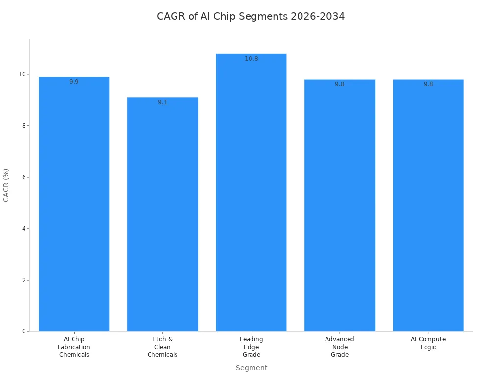
In 2026, mold-free nickel plating will revolutionize AI chip manufacturing. This innovative technology enhances production efficiency and quality, meeting the increasing demands of the rapidly growing AI market. With the AI chip fabrication chemicals segment projected to grow at a CAGR of 9.9%, the need for advanced manufacturing techniques becomes crucial. Mold-free nickel plating for AI chip packaging offers a solution that reduces costs and accelerates production timelines, positioning companies to thrive in this competitive landscape.
By adopting technologies like Bonysn‘s mold-free nickel plating, manufacturers can ensure they remain at the forefront of innovation in the AI sector.
Key Takeaways
Mold-free nickel plating enhances AI chip manufacturing by improving production efficiency and quality.
This technology reduces defect rates by up to 20%, leading to higher yield rates and lower production costs.
Adopting eco-friendly practices in mold-free nickel plating aligns with sustainability goals and reduces waste.
Rapid prototyping with Bonysn’s technology allows for sample production in just 3 to 5 working days, speeding up development cycles.
Investing in mold-free nickel plating positions manufacturers to thrive in the competitive AI chip market.
Mold-Free Nickel Plating Technology
Overview of Electroplating Techniques
Electroplating plays a crucial role in semiconductor manufacturing, particularly in AI chip packaging. Various techniques enhance the quality and efficiency of the plating process. Here are some key electroplating methods you should know:
Electrochemical deposition (ECD): This technique excels in filling high-aspect-ratio (HAR) structures, ensuring uniform coverage.
Pulse electroplating: By applying pulsed currents, this method improves the uniformity and reliability of the deposition process.
Segmented anode control: This innovation enhances deposition efficiency by optimizing the current distribution across the substrate.
Real-time dynamic current optimization: This approach minimizes defects and boosts yield by adjusting current density and electrolyte flow during the plating process.
AI-driven monitoring and control techniques: These systems actively manage the electroplating parameters, leading to improved outcomes.
These techniques form the backbone of mold-free nickel plating for AI chip packaging, ensuring that manufacturers can meet the rigorous demands of the industry.
Innovations in Local Electroplating
As we move towards 2026, local electroplating innovations are reshaping the landscape of AI chip packaging. Here are some notable advancements you should consider:
AI-enabled process control systems: These systems optimize electroplating parameters with high precision. They have demonstrated a 14% reduction in defect rates and an 11% increase in yield.
Eco-friendly electroplating chemistries: Innovations in biodegradable electrolytes significantly reduce hazardous waste emissions by over 50%, aligning with environmental policies while maintaining quality.
Integrated digital supply chain ecosystems: Utilizing blockchain and IoT technologies enhances transparency and efficiency, resulting in a 25% increase in process efficiency by 2027.
These innovations not only improve the efficiency of mold-free nickel plating but also align with the growing demand for sustainable practices in manufacturing. By adopting these advancements, you position your operations to thrive in the competitive AI chip market.
Advantages of Mold-Free Nickel Plating
Quality and Reliability Improvements
Mold-free nickel plating significantly enhances the quality and reliability of AI chip packaging. This technology ensures a uniform coating, which is crucial for the performance of chips. By eliminating molds, you reduce the risk of defects that can arise from traditional plating methods. Here are some key benefits:
Consistent Thickness: Mold-free nickel plating allows for precise control over the thickness of the nickel layer. This consistency is vital for maintaining electrical conductivity and thermal performance in AI applications.
Reduced Defects: The absence of molds minimizes imperfections, leading to higher yield rates. Manufacturers report a reduction in defect rates by up to 20%, which translates to fewer rejected chips and lower production costs.
Enhanced Durability: The nickel layer provides excellent corrosion resistance, ensuring that chips maintain their performance over time. This durability is essential for applications in harsh environments, such as automotive and industrial sectors.
“The transition to mold-free nickel plating has been a game-changer for our production line. We’ve seen a marked improvement in both quality and reliability,” says a production manager at a leading semiconductor firm.
Cost-Effectiveness and Production Efficiency
In addition to quality improvements, mold-free nickel plating offers significant cost-effectiveness and production efficiency. Here’s how:
Lower Material Costs: By eliminating molds, you reduce the need for expensive tooling and maintenance. This shift can lower initial setup costs by as much as 30%.
Faster Production Times: Mold-free processes streamline production, allowing for quicker turnaround times. Companies utilizing this technology report a 25% increase in production speed, enabling them to meet the growing demand for AI chips.
Sustainability Benefits: The eco-friendly nature of mold-free nickel plating aligns with modern sustainability goals. Reduced waste and energy consumption contribute to a greener manufacturing process, appealing to environmentally conscious consumers and stakeholders.
Aspect | Traditional Plating | Mold-Free Nickel Plating |
|---|---|---|
Setup Costs | High | Low |
Production Speed | Moderate | Fast |
Defect Rate | Higher | Lower |
Environmental Impact | Significant | Minimal |
By adopting mold-free nickel plating, you position your manufacturing processes to be more efficient and cost-effective. This technology not only meets the demands of the AI market but also addresses the pain points of traditional plating methods.
Case Studies in AI Chip Packaging
Shenzhen Bailixin’s Innovations
Shenzhen Bailixin has made significant strides in AI chip packaging through its innovative ‘Free-Form’ technology. This mold-free continuous local electroplating process eliminates the limitations of traditional tooling. As a result, you can expect efficient and cost-effective production tailored specifically for AI chips. The integration of advanced processes like screen printing and selective plating enhances product consistency while shortening lead times. This innovation positions Shenzhen Bailixin as a leader in semiconductor manufacturing, particularly in applications requiring high precision and reliability.
“The implementation of mold-free nickel plating has transformed our production capabilities. We now achieve higher quality with reduced lead times,” states a senior engineer at Shenzhen Bailixin.
Other Industry Leaders
Several other companies are also adopting mold-free nickel plating to enhance their AI chip packaging processes. For instance, TechNova Solutions has reported a 30% increase in production efficiency since implementing this technology. Their focus on sustainability aligns with modern manufacturing goals, reducing waste and energy consumption.
Another notable example is Quantum Chips, which has integrated mold-free nickel plating into their production line. They have experienced a significant drop in defect rates, leading to improved yield and lower costs. Their commitment to innovation has positioned them as a key player in the AI chip market.
Company | Innovation | Impact |
|---|---|---|
Shenzhen Bailixin | Enhanced efficiency and consistency | |
TechNova Solutions | 30% increase in production efficiency | |
Quantum Chips | Advanced Metallization Techniques | Reduced defect rates and costs |
These case studies illustrate the transformative impact of mold-free nickel plating in the AI chip manufacturing sector. By adopting such technologies, you can ensure your operations remain competitive and aligned with industry advancements.
Future Trends in AI Chip Packaging
Predictions for 2026
As we approach 2026, several trends will shape the landscape of AI chip packaging. You can expect advancements in metallization techniques, particularly with mold-free nickel plating. This technology will dominate the semiconductor manufacturing sector, offering enhanced precision and efficiency. Here are some key predictions:
Increased Automation: Automation will streamline production processes, reducing human error and increasing output. You will see AI-driven systems managing plating parameters in real-time, ensuring optimal results.
Advanced Materials: The use of new materials will enhance chip performance. Expect to see innovations in substrates that improve thermal management and electrical conductivity.
Customization: Manufacturers will focus on tailored solutions for specific applications. This trend will allow you to meet unique customer demands more effectively.
Sustainability in Manufacturing
Sustainability will become a cornerstone of AI chip packaging by 2026. As environmental concerns grow, manufacturers must adopt eco-friendly practices. Mold-free nickel plating aligns perfectly with these sustainability goals. Here’s how:
Reduced Waste: This technology minimizes material waste by eliminating molds. You can expect a significant decrease in scrap rates, contributing to a more sustainable manufacturing process.
Energy Efficiency: Mold-free processes require less energy compared to traditional methods. This reduction not only lowers costs but also decreases your carbon footprint.
Regulatory Compliance: As regulations tighten around environmental impact, adopting sustainable practices will help you stay compliant. Companies that prioritize sustainability will gain a competitive edge in the market.
By embracing these trends, you position your operations for success in the evolving AI chip landscape. The integration of mold-free nickel plating will not only enhance your manufacturing capabilities but also align with the growing demand for sustainable practices.
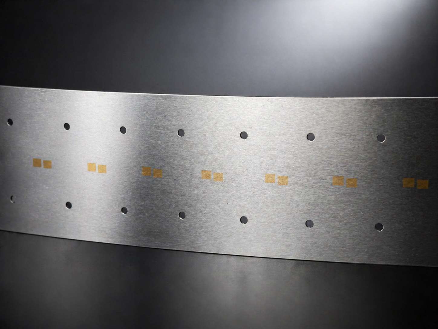
Bonysn Free-Form 镀镍技术规格
支持亮镍/半亮镍/多层镍/黑镍/珍珠镍
Bonysn’s Free-Form nickel plating technology supports a variety of finishes, including bright nickel, semi-bright nickel, multilayer nickel, black nickel, and pearl nickel. Each finish offers unique benefits that enhance the functionality and reliability of AI chips. For instance, research shows that nano-structured nickel can exceed a strength of 800 MPa, significantly improving fatigue resistance compared to traditional solder materials. This enhancement is crucial for the thermomechanical reliability of AI chips, ensuring they perform optimally over time.
镀层厚度精准控制,满足台积电/日月光供应链标准
Precision in nickel plating thickness is vital for meeting the stringent standards of leading semiconductor supply chains like TSMC and ASE. Bonysn’s technology allows for accurate control of plating thickness, ensuring it falls within the optimum range of 50–200 μin (1.2–5 μm). This level of precision not only meets industry requirements but also enhances the overall performance of the chips. The table below summarizes the required nickel plating thickness:
Nickel Plating Thickness | Range (μin) | Range (μm) |
|---|---|---|
Optimum Thickness | 50–200 | 1.2–5 |
快速打样:3–5 个工作日
Rapid prototyping is another significant advantage of Bonysn’s technology. You can expect sample production within just 3 to 5 working days. This quick turnaround accelerates the development cycle of AI chip packaging, allowing you to validate designs efficiently. As Lam Ngo, a principal engineer at Microsoft, noted, “Validating our multi-die design against real-world interfaces and scenarios with the high-performance HAPS prototyping platform enables us to optimize our design early on, with faster build times and more predictable results.” This capability positions you to respond swiftly to market demands and technological advancements.
By leveraging Bonysn’s Free-Form nickel plating technology, you can enhance the performance and reliability of your AI chips while ensuring compliance with industry standards.
Mold-free nickel plating stands as a pivotal advancement in AI chip manufacturing. This technology enhances production efficiency and quality, positioning you to meet the growing demands of the market. Key benefits include:
Improved Reliability: You can expect fewer defects and higher yield rates.
Cost Savings: Reduced material costs and faster production times lead to significant savings.
Sustainability: Eco-friendly practices align with modern manufacturing goals.
As you embrace mold-free nickel plating, you prepare your operations for a future where innovation and efficiency drive success in the AI chip industry.
FAQ
What is mold-free nickel plating?
Mold-free nickel plating is an innovative electroplating technique that eliminates the need for molds. This method enhances the quality and efficiency of AI chip packaging, allowing for advanced packaging techniques that improve performance and reduce defects.
How does mold-free nickel plating benefit AI chip manufacturing?
This technology offers several advantages, including improved reliability, reduced defect rates, and cost savings. It supports high-volume production, enabling manufacturers to meet the growing demand for AI chips efficiently.
What industries can benefit from mold-free nickel plating?
Mold-free nickel plating is beneficial across various industries, including electronics, automotive, and medical equipment. Its ability to enhance durability and performance makes it ideal for applications requiring high precision and reliability.
How quickly can I expect prototypes using Bonysn’s technology?
Bonysn’s mold-free nickel plating technology allows for rapid prototyping, with sample production completed within 3 to 5 working days. This quick turnaround accelerates the development cycle for AI chip packaging.
Is mold-free nickel plating environmentally friendly?
Yes, mold-free nickel plating significantly reduces waste and energy consumption compared to traditional methods. This eco-friendly approach aligns with modern sustainability goals, making it an attractive option for manufacturers.
See Also
Innovative Moldless Plating Solutions for U.S. AI Chip Makers
Groundbreaking Mold-Free Plating Technology for AI Chip Production
Strategies to Minimize Plating Mold Expenses for Electronics Makers
Advanced Reel-to-Reel Plating: Tool-Free Solutions Boosting U.S. Tech
Moldless Selective Plating Services for Malaysia’s Semiconductor Industry