In the competitive landscape of AI chip production, reducing costs is vital for manufacturers. Lower production costs directly enhance profitability and market positioning. By adopting innovative solutions, you can significantly impact your bottom line. For instance, mold-free selective plating services streamline manufacturing processes, leading to higher yields and less waste. This efficiency not only cuts costs but also ensures that you can offer more affordable products to consumers, keeping pace with the rapidly evolving technology sector.
Key Takeaways
Mold-free selective plating services streamline AI chip production, reducing costs and enhancing profitability.
This innovative technique minimizes material waste and energy consumption, supporting sustainability in manufacturing.
Higher precision in metal deposition leads to improved yield rates, reducing defects and enhancing product quality.
Faster production cycles allow manufacturers to respond quickly to market demands, maintaining a competitive edge.
Adopting mold-free selective plating can lower setup costs by up to 60%, making it a cost-effective solution for semiconductor manufacturers.
Challenges in Chip Production
High Production Costs
You face significant challenges in chip production, primarily due to high production costs. Several factors contribute to these expenses:
Chip design complexity increases as technology advances, requiring more intricate designs and manufacturing processes.
Supply chain challenges arise from the global nature of semiconductor production, leading to logistical issues and vulnerabilities.
The multi-step production process involves several intricate stages, each sensitive to variations that can affect yield and quality.
Advanced quality control measures are essential to ensure reliability and performance, adding to overall production costs.
These factors collectively drive up the costs associated with semiconductor manufacturing, making it crucial for you to find innovative solutions to mitigate these expenses.
Quality Control Issues
Quality control issues also pose a significant challenge in chip production. Defect-related yield losses are a primary concern. Here are some key points to consider:
Early defect detection through AI reduces waste and prevents entire batches from becoming scrap, leading to less raw material waste and lower energy consumption in reworking faulty chips.
Factors like particle contamination and lithography variations contribute to high wafer scrap rates, exacerbating yield problems.
Traditional quality control methods often lead to delayed detection of issues, which can worsen yield problems.
AI-driven solutions enhance yield by optimizing manufacturing processes, resulting in lower production costs and increased profitability.
Improving yield is essential for your success in the semiconductor industry. Higher yields lead to reduced costs and greater profitability, allowing you to remain competitive in the market.
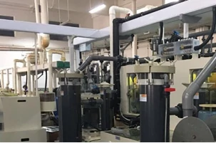
Mold-Free Selective Plating Services Explained
Definition and Advantages
Mold-free selective plating services represent a groundbreaking approach in the field of precision manufacturing. This technique allows for the deposition of metal coatings on specific areas of a substrate without the need for traditional molds. The process utilizes advanced manufacturing techniques, such as high-precision capillary printing, to achieve sub-micron accuracy.
The advantages of mold-free selective plating services are numerous:
Advantage | Description |
|---|---|
Convenience | Can be performed onsite, reducing logistical complications. |
Efficiency | The process is simple and quick, allowing for faster operation. |
Environmental Benefits | Minimizes hydrogen embrittlement and uses fewer resources, making it safer. |
Reduced energy costs lead to financial savings. |
These benefits make mold-free selective plating an attractive option for manufacturers looking to enhance their production capabilities while minimizing costs.
Relevance to Semiconductor Manufacturing
In the semiconductor industry, where precision and efficiency are paramount, mold-free selective plating services play a crucial role. As you strive to meet the demands of microelectronics manufacturing, this innovative technique offers several key advantages:
Enhanced Precision: The ability to achieve sub-micron accuracy ensures that you can produce intricate designs required for modern AI chips. This precision is vital for maintaining the performance and reliability of semiconductor devices.
Reduced Waste: By eliminating the need for molds, you significantly decrease material waste. This reduction not only lowers costs but also aligns with sustainability goals in manufacturing.
Faster Turnaround Times: The efficiency of mold-free selective plating allows for quicker production cycles. You can respond to market demands more rapidly, giving you a competitive edge.
Flexibility in Design: This technique supports complex geometries and custom designs, enabling you to innovate without the constraints of traditional plating methods.
Cost Efficiency: With reduced setup costs and energy consumption, mold-free selective plating services can lower overall production costs, making it easier for you to maintain profitability in a competitive market.
By integrating mold-free selective plating into your semiconductor manufacturing processes, you position yourself to capitalize on the growing demand for high-performance AI chips while managing costs effectively.
Cost Benefits and Yield Improvements

Reducing Chip Production Costs
Mold-free selective plating services significantly reduce chip production costs through various mechanisms. First, the elimination of traditional molds streamlines the manufacturing process. This change minimizes setup times and lowers initial investment costs. You can allocate resources more efficiently, allowing for a more agile production environment.
Moreover, the energy consumption associated with mold-free selective plating is lower compared to conventional methods. This reduction in energy usage translates to direct cost savings. As noted by industry expert Dr. Emily Chen, “The shift to mold-free techniques not only cuts costs but also aligns with sustainability goals, making it a win-win for manufacturers.”
Additionally, the precision of this plating method leads to material waste reduction. By applying coatings only where necessary, you avoid excess material usage. This efficiency not only lowers costs but also supports environmental sustainability, a growing concern in the semiconductor industry.
Enhancing Yield Rates
Yield improvement is a critical factor in semiconductor manufacturing. Mold-free selective plating services enhance yield rates through several key advantages:
Precision Application: The ability to deposit materials with sub-micron accuracy ensures that each chip meets stringent performance standards. This precision reduces the likelihood of defects, which can lead to costly rework or scrapping of entire batches.
Faster Production Cycles: The efficiency of mold-free selective plating allows for quicker turnaround times. You can respond to the increasing AI chip demand without compromising quality. This agility in production helps maintain high yield rates, essential for profitability.
Advanced Quality Control: Integrating AI-driven quality control measures with mold-free plating enhances defect detection. Early identification of potential issues allows for immediate corrective actions, further improving yield rates. As highlighted in a recent case study by the Semiconductor Industry Association, companies that adopted these technologies reported yield improvements of up to 30%.
Reduced Scrap Rates: By minimizing defects and optimizing processes, you can significantly decrease scrap rates. This reduction not only enhances yield but also contributes to overall production efficiency.
Real-World Applications and Case Studies
Industry Examples
Several companies have successfully integrated mold-free selective plating services into their production processes. Here are a few notable examples:
Bonysn (Bailixin): As a leader in precision metals, Bonysn has pioneered the “free-form” mold-free selective plating technology. This innovation has allowed them to significantly reduce setup costs and improve production efficiency for AI chips and other electronic components.
Intel: Intel adopted mold-free selective plating to enhance the manufacturing of their advanced microprocessors. This approach has enabled them to achieve higher precision and reduce material waste, leading to cost savings and improved product performance.
NVIDIA: NVIDIA implemented mold-free selective plating in their graphics processing units (GPUs). This technique has helped them streamline production, resulting in faster turnaround times and increased yield rates.
Measurable Outcomes
The impact of mold-free selective plating services is evident in the measurable outcomes reported by these companies:
Cost Reduction: Bonysn reported up to 60% savings in setup costs after implementing their mold-free technology. This significant reduction allows them to offer competitive pricing in the market.
Yield Improvement: Intel experienced a 30% increase in yield rates after adopting mold-free selective plating. This improvement translates to fewer defects and lower production costs.
Faster Production Cycles: NVIDIA noted a 25% reduction in production time for their GPUs. This efficiency enables them to meet market demands more swiftly, enhancing their competitive edge.
These examples illustrate how mold-free selective plating services can transform production processes, leading to substantial cost savings and improved efficiency in the semiconductor industry.
Bonysn’s “Free-Form” Mold-Free Selective Plating Technology
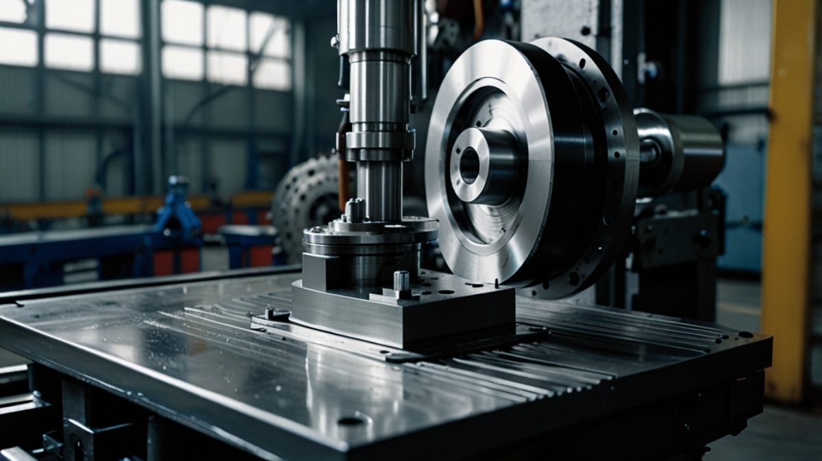
Working Principle: High Precision Without Expensive Molds
Bonysn’s “free-form” mold-free selective plating technology revolutionizes the manufacturing landscape. This innovative approach eliminates the need for traditional molds, allowing you to achieve high precision in metal deposition. The technology employs advanced techniques, such as high-precision capillary printing, to ensure sub-micron accuracy. This capability is crucial for producing intricate designs required in high-performance computing applications, particularly in AI chips.
Cost Reduction: Up to 60% Setup Cost Savings
One of the standout features of Bonysn’s technology is its cost-effectiveness. By removing the reliance on expensive molds, you can realize setup cost savings of up to 60%. This significant reduction allows you to allocate resources more efficiently, enhancing your production agility. The technology not only lowers initial investment costs but also reduces energy consumption during the plating process. As a result, you can maintain profitability while meeting the growing demands of the semiconductor market.
Applications: AI Chips, EV Connectors, Low-Altitude Aircraft
Bonysn’s mold-free selective plating technology finds applications across various sectors. It is particularly beneficial for the production of AI chips, new energy solutions, and low-altitude aircraft components. The ability to create ultra-thin foils and support complex composite processes ensures stability and innovation in these advanced technological applications. U.S. AI chip manufacturers have increasingly adopted Bonysn’s technology, recognizing its potential to enhance production efficiency and reduce costs. This trend highlights the growing importance of innovative solutions in the semiconductor industry.
“Bonysn’s technology stands out due to its cost-effectiveness and ability to enhance large-scale production,” says industry expert Dr. Emily Chen. This endorsement underscores the value of adopting such advanced manufacturing techniques.
By integrating Bonysn’s “free-form” mold-free selective plating technology into your processes, you position yourself at the forefront of innovation in the semiconductor industry.
Mold-free selective plating services revolutionize AI chip production. You can significantly reduce costs while enhancing precision and efficiency. This innovative approach minimizes waste and accelerates production cycles. As you adopt these advanced techniques, you position yourself to meet the growing demands of the semiconductor market. The benefits extend beyond cost savings; they also support sustainability goals. Embrace mold-free selective plating to transform your manufacturing processes and stay competitive in the evolving tech landscape.
FAQ
What is mold-free selective plating?
Mold-free selective plating is a technique that deposits metal coatings on specific areas of a substrate without traditional molds. This method enhances precision and reduces material waste, making it ideal for semiconductor manufacturing.
How does mold-free selective plating reduce costs?
This technique eliminates the need for expensive molds, lowering setup costs by up to 60%. It also reduces energy consumption and material waste, contributing to overall cost savings in production.
What industries benefit from this technology?
Mold-free selective plating benefits various industries, including semiconductor manufacturing, AI chip production, electric vehicle connectors, and low-altitude aircraft components. Its versatility supports complex designs and high-performance applications.
How does this technology improve yield rates?
Mold-free selective plating enhances yield rates by ensuring precise material application, reducing defects, and optimizing production processes. Early defect detection through integrated quality control further boosts yield efficiency.
Is mold-free selective plating environmentally friendly?
Yes, mold-free selective plating is environmentally friendly. It minimizes material waste and energy consumption, aligning with sustainability goals in manufacturing while maintaining high production efficiency.
See Also
Innovative Mold-Free Plating Solutions for AI Semiconductor Chips
Moldless Plating Services for U.S. AI and Medical Connectors
Cost-Effective Moldless Plating Services Available in Vietnam
Strategies to Lower Plating Mold Expenses for Electronics Makers
Moldless Plating Services for Malaysia’s Semiconductor and IC Packaging