
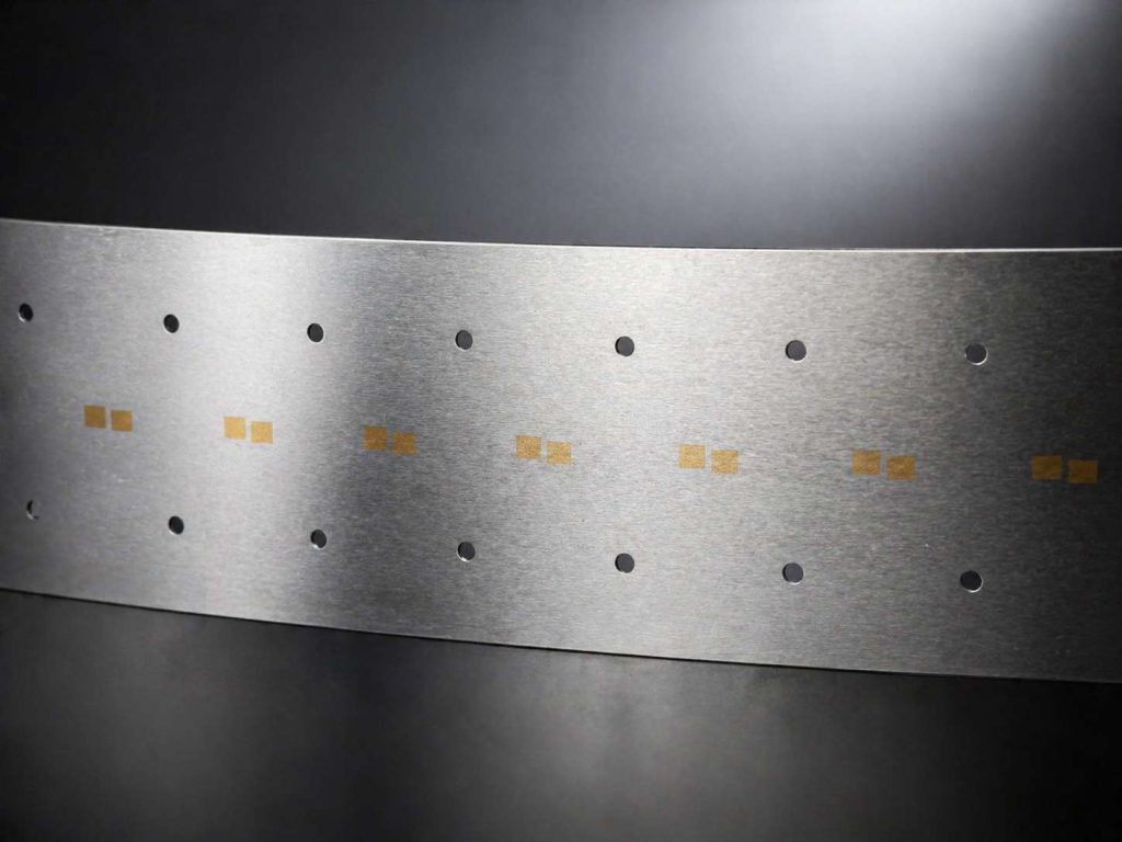
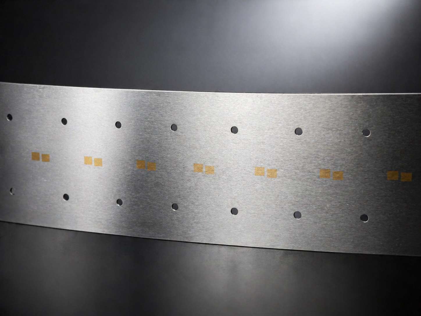
Precision stainless steel strips play a vital role in the semiconductor packaging industry. You rely on these strips for their efficiency and reliability in manufacturing processes. As the demand for high-quality materials grows in Malaysia’s semiconductor sector, the importance of using durable and precise components becomes increasingly clear. Manufacturers like you benefit from the enhanced performance and lower defect rates that these strips provide, making them essential in today’s competitive landscape.
Key Takeaways
Precision stainless steel strips are essential for semiconductor packaging, enhancing efficiency and reliability in manufacturing.
Understanding the material composition, like chromium and nickel content, helps you choose the right stainless steel strips for your needs.
Tight tolerances of ±0.005 mm ensure a perfect fit in designs, reducing defects and improving product quality.
BonySN’s advanced etching technology streamlines production, lowers costs, and enhances thermal management in semiconductor devices.
The semiconductor packaging market in Malaysia is expected to grow significantly, making it important to stay updated on material innovations.
Characteristics of Stainless Steel Strips
Material Composition
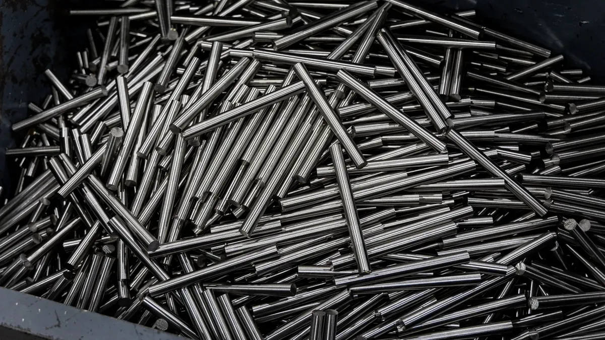
Understanding the material composition of stainless steel strips is crucial for their application in the semiconductor packaging industry. Stainless steel strips typically consist of iron, chromium, and nickel. The chromium content, usually between 10.5% and 30%, provides corrosion resistance. Nickel enhances ductility and toughness, making the strips easier to work with during manufacturing processes.
You may also encounter various grades of stainless steel, such as 304 and 316. Grade 304 is widely used due to its excellent corrosion resistance and formability. In contrast, grade 316 offers superior resistance to pitting and is ideal for harsher environments. The microstructure of these materials can significantly affect their performance. For instance, austenitic stainless steels, which contain high levels of nickel, exhibit better formability and weldability compared to ferritic types.
Dimensions and Tolerances
When it comes to dimensions and tolerances, precision is key. Stainless steel strips come in various thicknesses, typically ranging from 0.01 mm to 2.0 mm. This range allows you to select the right thickness for your specific application. The width of these strips can vary as well, often falling between 3 mm and 300 mm, depending on the requirements of your manufacturing process.
Tolerances are equally important. You should expect tolerances as tight as ±0.005 mm for high-precision applications. This level of accuracy ensures that the stainless steel strips fit perfectly into your semiconductor packaging designs, minimizing defects and enhancing overall product quality.
To illustrate the importance of these characteristics, consider the following comparison table:
Grade | Corrosion Resistance | Ductility | Typical Thickness Range (mm) |
|---|---|---|---|
304 | Good | Excellent | 0.01 – 2.0 |
316 | Excellent | Good | 0.01 – 2.0 |
Applications in Semiconductor Packaging

Lead Frames
Lead frames serve as critical components in semiconductor packaging. They provide the necessary electrical connections between the semiconductor chip and the external circuit. You often use stainless steel strips for lead frames due to their excellent conductivity and mechanical strength. The durability of these strips ensures that they can withstand the stresses of manufacturing and operation.
Using precision stainless steel strips in lead frames offers several advantages:
Enhanced Electrical Performance: The high conductivity of stainless steel strips ensures efficient signal transmission.
Corrosion Resistance: The chromium content in stainless steel protects against oxidation, extending the lifespan of lead frames.
Customizability: You can easily modify the dimensions and shapes of stainless steel strips to meet specific design requirements.
Thermal Management
Effective thermal management is essential in semiconductor packaging. As devices become smaller and more powerful, managing heat becomes increasingly important. Stainless steel strips play a vital role in dissipating heat away from sensitive components. Their thermal conductivity helps maintain optimal operating temperatures, preventing overheating and ensuring reliability.
BonySN’s etching technology significantly enhances the functionality of stainless steel strips for thermal management. This technology allows for precise etching without the need for mold opening, which accelerates production and improves flexibility. Here are some key features of BonySN’s etching technology:
Feature | Description |
|---|---|
Quick Sample Making | No mold opening required |
Precision | Maximum precision of ±0.005mm |
Processing Thickness | 0.01 – 2.0 mm |
Enhancements | Facilitates stamping, bending, electroplating, and injection molding |
Efficiency Improvement | Significantly improves efficiency, reduces costs, and lowers defect rates |
By integrating this advanced etching technology into your production line, you can expect improved thermal management solutions. The ultra-clean surfaces produced by BonySN’s process minimize the risk of residual oil and metal impurities, which are common pain points in wafer foundries. This attention to detail ensures that your semiconductor packaging meets the highest industry standards.
In regions like Penang and Kuala Lumpur, the demand for solid crystal clamps, lead frames, and fixtures continues to grow. As you navigate this competitive landscape, leveraging the advantages of precision stainless steel strips and innovative technologies like those from BonySN can set you apart from the competition.
Advantages of Precision Stainless Steel Strips
Durability
Precision stainless steel strips are known for their exceptional durability. You can rely on these strips to withstand harsh manufacturing environments and prolonged operational use. Their high chromium content provides excellent resistance to corrosion, ensuring that the material remains intact even in challenging conditions. This makes them ideal for semiconductor packaging, where reliability is critical.
The mechanical strength of stainless steel strips also contributes to their durability. They resist deformation under stress, maintaining their structural integrity during processes like stamping, bending, and injection molding. For example, BonySN’s roll-to-roll continuous etching technology enhances the durability of these strips by producing ultra-clean surfaces with zero burrs. This precision minimizes weak points, reducing the likelihood of material failure.
Performance Metrics
When it comes to performance, precision stainless steel strips excel in several key areas. Their tight tolerances, often as precise as ±0.005 mm, ensure a perfect fit in semiconductor packaging applications. This level of accuracy reduces assembly errors and enhances the overall quality of your products.
Cost efficiency is another significant advantage. By using high-precision materials, you can lower defect rates and minimize waste. BonySN’s advanced etching process further improves performance by streamlining production and reducing lead times. For instance, the ability to process thicknesses ranging from 0.01 mm to 2.0 mm allows you to meet diverse application needs without compromising on quality.
In addition, the thermal and electrical conductivity of stainless steel strips supports efficient heat dissipation and signal transmission. These properties are essential for maintaining the performance and longevity of semiconductor devices. By integrating precision stainless steel strips into your production line, you can achieve a balance of durability, efficiency, and cost-effectiveness.
bonysn’s stainless steel band
high-precision machining
BonySN’s stainless steel band features high-precision machining that sets it apart in the semiconductor packaging industry. You can expect a remarkable precision level of ±0.005 mm. This accuracy ensures that the strips fit perfectly into your designs, reducing assembly errors. The advanced machining techniques used by BonySN allow for intricate designs and shapes, catering to your specific needs.
The surface coating is uniform
Uniform surface coating is another hallmark of BonySN’s stainless steel band. A consistent coating enhances the corrosion resistance of the strips. This feature is crucial for maintaining the integrity of semiconductor packages over time. The uniformity also contributes to better adhesion during processes like electroplating and bonding. You can trust that BonySN’s meticulous attention to surface quality will lead to higher performance in your applications.
Continuous roll-to-roll production
BonySN employs a continuous roll-to-roll production method, which streamlines the manufacturing process. This technique allows for efficient processing of stainless steel strips, minimizing waste and reducing lead times. You benefit from faster production cycles and lower costs. The roll-to-roll method also supports various thicknesses, ranging from 0.01 mm to 2.0 mm, making it versatile for different applications.
Feature | Benefit |
|---|---|
High-Precision Machining | Reduces assembly errors with ±0.005 mm accuracy |
Uniform Surface Coating | Enhances corrosion resistance and adhesion |
Continuous Roll-to-Roll Production | Minimizes waste and lowers production costs |
By choosing BonySN’s stainless steel band, you gain access to cutting-edge technology that enhances your manufacturing capabilities. This commitment to quality and efficiency positions you for success in the competitive semiconductor packaging market.
Trends and Future Outlook in Malaysia
Innovations in Material Science
You will notice significant innovations in material science that impact the semiconductor packaging industry. Researchers focus on developing advanced alloys and composites that enhance the performance of stainless steel strips. For instance, new coatings improve corrosion resistance and thermal conductivity. These advancements allow you to create more efficient and reliable semiconductor packages.
Nanotechnology: This technology enhances material properties at the molecular level, leading to stronger and lighter components.
Smart Materials: These materials adapt to environmental changes, improving the functionality of semiconductor devices.
BonySN actively participates in these innovations, integrating cutting-edge etching technologies to produce high-quality stainless steel strips. Their precision etching process allows for rapid prototyping and customization, meeting the evolving demands of the industry.
Market Growth Projections
The semiconductor packaging market in Malaysia is poised for substantial growth. According to a recent report by the Malaysian Investment Development Authority (MIDA), the industry is expected to grow at a compound annual growth rate (CAGR) of 8.5% from 2023 to 2028. This growth is driven by increasing demand for electronic devices and advancements in manufacturing technologies.
Year | Market Size (USD Billion) | CAGR (%) |
|---|---|---|
2023 | 5.2 | 8.5 |
2028 | 7.8 | 8.5 |
As you consider your position in this expanding market, leveraging innovations in material science will be crucial. By adopting advanced materials and technologies, you can enhance your product offerings and stay competitive.
Tip: Keep an eye on emerging trends in material science. Staying informed will help you adapt and thrive in the evolving semiconductor landscape.
In summary, precision stainless steel strips play a crucial role in Malaysia’s semiconductor packaging industry. Their durability, high precision, and excellent thermal management capabilities enhance manufacturing efficiency. You can leverage BonySN’s innovative etching technology to improve your production processes. As the industry evolves, consider exploring advancements in material science and manufacturing techniques. These areas hold potential for further research and development, ensuring you stay competitive in this dynamic market.
FAQ
What are precision stainless steel strips used for in semiconductor packaging?
Precision stainless steel strips are essential for lead frames and thermal management in semiconductor packaging. They provide electrical connections and help dissipate heat, ensuring reliable device performance.
How does BonySN’s etching technology improve production?
BonySN’s etching technology allows for precision etching without mold opening. This accelerates production, enhances flexibility, and ensures high-quality results with minimal defects.
What are the benefits of using stainless steel strips over other materials?
Stainless steel strips offer superior durability, corrosion resistance, and excellent thermal and electrical conductivity. These properties make them ideal for demanding semiconductor applications.
How do I choose the right thickness for stainless steel strips?
Select the thickness based on your specific application requirements. Stainless steel strips typically range from 0.01 mm to 2.0 mm, allowing you to find the perfect fit for your needs.
What is the expected market growth for the semiconductor packaging industry in Malaysia?
The semiconductor packaging market in Malaysia is projected to grow at a CAGR of 8.5% from 2023 to 2028, driven by increasing demand for electronic devices and advancements in manufacturing technologies.
See Also
Enhancing Electronics With Precision Metal Strip Materials
Selective Plating Solutions Without Molds for Malaysian Semiconductors
Boosting Smart Wearables With High-Precision Stainless Steel Strips
Etched Stainless Steel Springs: The Future of Medical Devices