
In today’s fast-paced electronics manufacturing landscape, precision metal strips are vital for minimizing pitch and maximizing yield in semiconductor applications. These components are essential for meeting the growing demand for miniaturized electronic devices.
The precision strip market is expected to grow from $2.40 billion in 2024 to $2.58 billion in 2025, reflecting a CAGR of 7.5%.
This growth stems from the rising need for reliable semiconductor materials and high-speed communication tools.
As you explore the advancements in precision metal strips, you’ll appreciate their significance in enhancing device performance and reliability.
Key Takeaways
Precision metal strips are essential for connecting semiconductor devices to circuit boards, enhancing performance and reliability.
Minimizing pitch increases device density, but it can also lead to challenges like cell-to-cell interference; balance is key.
Advanced manufacturing techniques, such as pulse electroplating and etching, improve the quality and precision of metal strips.
Implementing robust quality control measures can significantly enhance yield rates and reduce defects in production.
Bonysn’s innovative approaches in material selection and manufacturing processes set a high standard for precision metal strips.
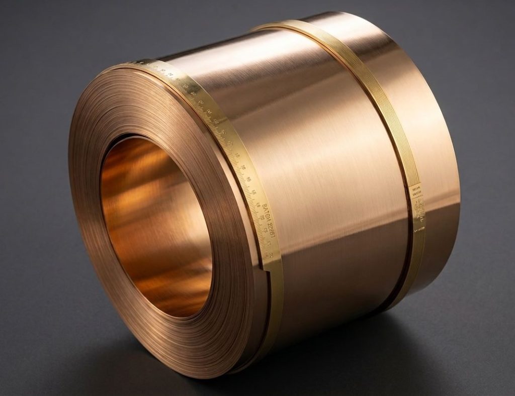
Precision Metal Strips Overview
Precision metal strips play a crucial role in the production of semiconductor lead frames. These strips serve as the foundation for connecting semiconductor devices to their respective circuit boards. Their design and manufacturing processes directly influence the performance and reliability of electronic components.
Composition and Materials
The materials used in precision metal strips significantly impact their properties and suitability for various applications. Here’s a breakdown of the primary materials and their respective characteristics:
Material | Properties |
|---|---|
Copper | Excellent electrical and thermal conductivity, affordable, easy to manufacture, good strength and flexibility. |
Copper Alloys | Improved mechanical properties, higher resistance to stress, suitable for demanding applications. |
Iron-Nickel Alloys | Matches thermal expansion of silicon, corrosion resistance, high mechanical strength. |
Stainless Steel | Good corrosion resistance, excellent durability, used in harsh environments. |
These materials ensure that precision metal strips can withstand the rigors of high-density applications while maintaining optimal performance.
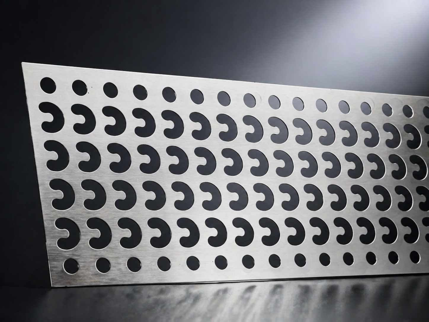
Manufacturing Techniques
The manufacturing techniques employed in producing precision metal strips are vital for achieving the desired quality and precision. Here are some common techniques used in the industry:
Bending
Drawing
Extrusion
Forging
Rolling
Stamping
Each technique has its advantages and is selected based on the specific application requirements. For instance, stamping is cost-effective for mass production, while etching offers high precision for complex geometries.
Advanced manufacturing processes contribute significantly to the consistency and accuracy of metal strips. Techniques such as CNC machining, EDM (Electrical Discharge Machining), and laser cutting enhance the precision of the final product. These methods ensure that you achieve high accuracy and uniformity across high-pin-count designs.
Bonysn stands out in the industry by integrating innovative manufacturing processes. Their commitment to quality control and material selection ensures that every precision metal strip meets rigorous standards. This focus on excellence allows Bonysn to provide products that not only meet but exceed customer expectations.
By understanding the composition and manufacturing techniques of precision metal strips, you can appreciate their importance in semiconductor lead frames. These components are essential for enhancing device performance and reliability in today’s high-density electronic applications.
Importance of Pitch in Semiconductor Design
In semiconductor design, pitch refers to the distance between the centers of adjacent components. This measurement plays a crucial role in determining device density, which directly affects performance and efficiency. As you aim for higher density in your designs, understanding pitch becomes essential.
Impact on Device Density
Minimizing pitch allows for more components to fit within a given area, enhancing device density. For instance, high-density magnetic tunnel junction (MTJ) arrays with a pitch of 72 nm were successfully fabricated using a 1x nm DRAM platform. The critical dimension of the magnesium oxide (MgO) used in the MTJ array was only 30 nm, resulting in an impressive equivalent cell size of 0.0044 μm². This example illustrates how tighter pitch can lead to significant advancements in device capabilities.
However, reducing pitch also presents challenges. You may encounter issues such as cell-to-cell interference and lateral charge migration. These problems can negatively impact device performance, making it essential to balance density with reliability.
Alignment and Reliability
Precision in alignment is vital for the long-term reliability of semiconductor devices. You must ensure that alignment remains sub-nanometer to avoid defects. Even a single particle can cause significant damage to a chip, leading to costly failures. Hotspots can develop, degrading reliability over time.
Moreover, alignment issues can introduce yield risks during wafer-to-wafer bonding. Problems such as void formation in through-silicon vias (TSVs) can arise, affecting overall performance. Additionally, die shift during pick-and-place operations can lead to misalignment, while pressure-induced cracks during encapsulation can further compromise device integrity.
Advanced Techniques for Precision Metal Strips
In the realm of precision metal strips, innovations in manufacturing techniques play a pivotal role. You can significantly enhance the quality and performance of these strips through advanced electroplating and etching processes.
Electroplating and Etching Processes
Electroplating and etching are essential for achieving the desired precision in metal strips. Recent advancements in these processes have led to remarkable improvements:
Pulse electroplating enhances the quality and uniformity of deposited films. This technique is particularly beneficial for high aspect ratio (HAR) structures, ensuring consistent metal coverage.
It reduces mechanical stress in electroplated films, which is crucial for the reliability of advanced semiconductor nodes.
AI-driven monitoring optimizes electroplating parameters in real-time, improving precision and minimizing defects.
Continuous electroplating further boosts deposition rates and reduces defects. This results in higher quality and uniformity in metal strips. High-purity copper deposits minimize impurities, leading to smoother surfaces and fewer defects like V-pits. Advanced techniques, such as the Curvature-Enhanced-Accelerator Coverage (CEAC) mechanism, ensure rapid and uniform deposition, which is essential for high-density electronic applications.
Customization and Flexibility
Customization is key when it comes to precision metal strips. You can tailor these strips to meet specific project requirements, ensuring they fit seamlessly into your designs. The versatility of materials, such as stainless steel and copper alloys, allows for a wide range of applications.
Moreover, the ability to adjust thickness, width, and surface finish provides you with the flexibility needed for various industries. Whether you are working on mobile devices, medical equipment, or automotive components, precision metal strips can be adapted to suit your needs.
By leveraging these advanced techniques, you can enhance the performance and reliability of your semiconductor lead frames. The integration of innovative processes ensures that your products stand out in a competitive market.
Yield Maximization Strategies
Maximizing yield in semiconductor lead frame production involves strategic design considerations and rigorous quality control measures. By focusing on these areas, you can significantly enhance the efficiency and reliability of your manufacturing processes.
Design Considerations
When designing semiconductor lead frames, several critical factors influence yield rates. You should pay attention to the following aspects:
Lead Pitch: The spacing between electrical connections affects signal transmission and interference. A well-optimized lead pitch can enhance performance and reduce errors.
Lead Count: The number of leads determines the density of connections. Higher lead counts can complicate the package design but also increase functionality.
Frame Thickness: The thickness of the lead frame impacts mechanical stability and heat dissipation. A well-designed thickness ensures durability while maintaining optimal thermal management.
In terms of manufacturing techniques, consider the following methods based on your production volume:
Stamping: This method is the most economical for very high production volumes, allowing for rapid output.
Chemical Etching: Suitable for low to medium scale production runs, this technique offers lower tooling costs and allows for quick design optimizations without significant financial penalties.
Flexibility: Chemical etching provides significant advantages in production efficiency. It allows for rapid adaptations to tooling, ensuring consistent quality across large production runs.
By carefully selecting materials and optimizing designs, you can improve yield rates. For instance, transitioning from standard copper frames to custom copper-molybdenum composite frames can enhance yield by up to 11%. Additionally, addressing warpage during molding can directly impact efficiency and reject rates.
Quality Control Measures
Implementing robust quality control measures is essential for ensuring high yield and minimal defects in precision metal strip production. Here are some key practices to consider:
Quality Control Measure | Description |
|---|---|
Material certification review | Verify that the grade, chemistry, and mechanical properties meet specifications. |
Thickness and flatness checks | Ensure that coil or strip thickness and flatness are within tolerance for the die design. |
Surface condition | Check for scale, scratches, or contamination that could affect forming, coating, or conductivity. |
Scheduled die inspections | Regularly inspect cutting edges, forming features, and clearances. |
Preventive maintenance | Perform sharpening, polishing, and replacing wear components before they impact parts. |
First-article inspections | Validate new setups against drawings and requirements before releasing production. |
Statistical Process Control (SPC) | Track characteristic measurements over time to detect trends and correct processes. |
Fit and assembly checks | Verify that parts seat, engage, or latch correctly with mating components. |
Load and deflection testing | Ensure components that flex, support, or retain loads behave as designed. |
Advanced inspection technologies, such as machine vision systems, enhance defect detection and alignment. These systems can improve yield rates by 3-5% through early detection of process drift and pattern defects. Catching defects early minimizes manual inspection and rework, thus improving the production line yield rate per wafer.
By integrating these design considerations and quality control measures, you can maximize yield in semiconductor lead frame production. The combination of high-strength materials and efficient manufacturing processes, such as those offered by Bonysn, further enhances your ability to produce reliable and high-quality products.
Bonysn’s Breakthroughs in Precision Metal Strips
Bonysn leads the industry with its innovative approach to precision metal strips. Their commitment to advanced manufacturing techniques sets them apart from competitors. You can expect high-quality products that meet the rigorous demands of modern electronics.
Advanced Manufacturing Innovations
Bonysn employs cutting-edge technologies to enhance the production of precision metal strips. Techniques such as pulse electroplating and precision etching ensure that each strip meets stringent quality standards. These innovations not only improve the uniformity of coatings but also enhance the overall performance of the strips.
Diverse Material Portfolio
Bonysn offers a diverse range of materials for precision metal strips, each with unique properties that cater to various applications. The following table highlights some of the key materials in their portfolio:
Material Type | Unique Properties |
|---|---|
Stainless Steel Strips | Various model numbers (SUS301, SUS304, SUS305, SUS316, SUS430, N10, NM13) and applications in multiple industries (electronics, medical equipment, etc.) |
Pre-Plated Nickel | Used in high-precision applications and enhances corrosion resistance in various products. |
Special Copper Alloys | Offers excellent electrical conductivity and is suitable for electronic components. |
Continuous Electroplating | Provides a uniform coating that improves durability and performance of metal strips. |
High Strength and Performance
The precision metal strips from Bonysn exhibit exceptional strength and performance. Their materials are engineered to withstand harsh environments while maintaining optimal functionality. This reliability is crucial for applications in sectors such as automotive and aerospace.
Roll-to-Roll Processing & Integrated Techniques
Bonysn utilizes roll-to-roll processing, which allows for continuous production of precision metal strips. This method enhances efficiency and reduces waste, making it an environmentally friendly choice. Integrated techniques further streamline the manufacturing process, ensuring that you receive high-quality products consistently.
Broad Industry Applications
Bonysn’s precision metal strips find applications across various industries. From mobile devices to medical equipment, their products meet the diverse needs of modern manufacturing. This versatility makes Bonysn a trusted partner for businesses looking to enhance their product offerings.
By choosing Bonysn, you gain access to advanced solutions that elevate your manufacturing capabilities. Their breakthroughs in precision metal strips empower you to achieve higher performance and reliability in your electronic devices.
Case Studies and Applications
Successful Implementations
Precision metal strips have proven their value across various industries. For instance, in the automotive sector, manufacturers have successfully integrated these strips into battery contacts and spark plug terminals. This integration enhances performance and reliability, ensuring that vehicles operate efficiently.
In consumer electronics, companies utilize precision metal strips in devices like smartphones and digital cameras. These strips provide the high precision required for small parts, allowing for tighter tolerances and improved functionality.
Industry Applications
The versatility of precision metal strips extends to multiple industries. Here are some key sectors and their specific applications:
Automotive:
Clips
Spark plug terminals
Consumer Electronics:
Optical components in DVD players
Telecommunications:
EMI shields
Electronic contacts
The benefits of using precision metal strips are evident across these industries. The following table summarizes the advantages observed:
Industry | Benefits |
|---|---|
Automotive | Lightweight materials for automotive applications |
Electronics | High precision for electronic components |
Healthcare | Specialized materials for medical devices |
By adopting precision metal strips, companies can address market demands and customer pain points effectively. These strips not only enhance product performance but also contribute to the overall reliability of electronic devices.
In summary, advanced precision metal strips significantly enhance semiconductor lead frames and connectors. You benefit from several key advantages, including:
Precise accuracy and consistency, which minimize errors across large production volumes.
Flexibility for complex components, allowing intricate designs without sacrificing functionality.
Cost-efficiency at scale, enabling high-volume production at low unit costs.
Rapid prototyping and production, reducing time-to-market.
High levels of repeatability, ensuring consistent performance across millions of components.
Support for complex geometries and tight tolerances through advanced stamping techniques.
Integration with secondary operations, simplifying assembly processes.
By leveraging these benefits, you can improve manufacturing efficiency and product reliability in your electronic devices.
FAQ
What are precision metal strips used for in semiconductor applications?
Precision metal strips serve as the foundation for connecting semiconductor devices to circuit boards. They enhance performance and reliability in high-density electronic applications.
How does pitch affect semiconductor device performance?
Pitch determines the spacing between components. Minimizing pitch increases device density but can lead to challenges like cell-to-cell interference and alignment issues.
What materials are commonly used for precision metal strips?
Common materials include copper, copper alloys, iron-nickel alloys, and stainless steel. Each material offers unique properties suited for various applications.
How can I ensure high yield in production?
Focus on design considerations like lead pitch and frame thickness. Implement robust quality control measures to minimize defects and enhance overall yield.
What innovations does Bonysn offer in precision metal strips?
Bonysn utilizes advanced manufacturing techniques such as pulse electroplating and roll-to-roll processing. These innovations improve product quality and performance across various applications.
See Also
Enhancing Electronic Products With Precision Metal Strip Materials
Transforming Lead Frame Quality Through Selective Electroplating
Selective Plating Services Without Molds for Malaysian Semiconductor Packaging
Achieving ±0.005mm Precision in Semiconductor Metal Etching
Reducing Gold Plating Expenses in I/O Interfaces Using Selective Plating