
In the rapidly evolving world of semiconductors, the choice of materials for AI chiplet lead frames plays a crucial role. These materials directly influence performance and efficiency, impacting everything from processing speed to thermal management. By selecting the right AI chiplet lead frame materials, you can enhance the capabilities of your semiconductor devices. This selection process not only drives innovation but also ensures that your products meet the growing demands of modern technology.
Key Takeaways
Copper and aluminum are the most common materials for AI chiplet lead frames, each offering unique benefits in thermal conductivity and cost efficiency.
Advanced composites and alloys enhance thermal management and durability, making them ideal for high-performance semiconductor applications.
Precision etching techniques improve manufacturing accuracy, enabling intricate designs and reducing defects in AI chiplet lead frames.
Material innovations like embedded heat spreaders and laser-assisted stamping optimize cooling and signal integrity for AI processors.
Future trends in packaging focus on sustainability, advanced materials, and 3D integration to meet the growing demands of AI applications.
Lead Frame Materials
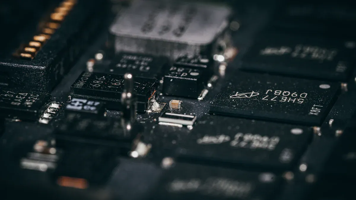
When selecting materials for AI chiplet lead frames, you typically encounter two common options: copper and aluminum. Each material has unique properties that make it suitable for specific applications in semiconductor manufacturing.
Common Materials
Copper: Known for its excellent thermal and electrical conductivity, copper is a popular choice for lead frames. Its high thermal conductivity allows for efficient heat dissipation, which is crucial in AI chiplet applications.
Aluminum: While aluminum has lower thermal conductivity than copper, it offers advantages in terms of weight and cost. This makes aluminum a viable option for applications where budget constraints are a concern.
Properties of Copper and Aluminum
The thermal conductivity of copper and aluminum significantly influences their performance in AI chiplet lead frames. The following table summarizes their thermal conductivity values:
Material | Thermal Conductivity (W/(m·K)) |
|---|---|
Copper | |
Aluminum | 237 |
As you can see, copper outperforms aluminum in thermal conductivity, making it ideal for high-performance applications. However, cost considerations often lead manufacturers to choose aluminum for its affordability. Lead frames account for about 14% of the semiconductor packaging market, emphasizing the importance of selecting cost-effective materials for high-volume production.
In addition to thermal properties, regulatory standards also impact material selection. The following table outlines key regulatory frameworks and their effects on lead frame materials:
Regulatory Framework | Impact on Material Selection |
|---|---|
RoHS | Mandates elimination of lead-based solders, promoting lead-free alternatives. |
REACH | Requires assessment of chemical substances, influencing material choices. |
WEEE | Encourages recycling and proper disposal of electronic waste, affecting packaging materials. |
Understanding these regulations helps you navigate the complexities of material selection for AI chiplet lead frames, ensuring compliance while optimizing performance.
Material Innovations
Composites and Alloys
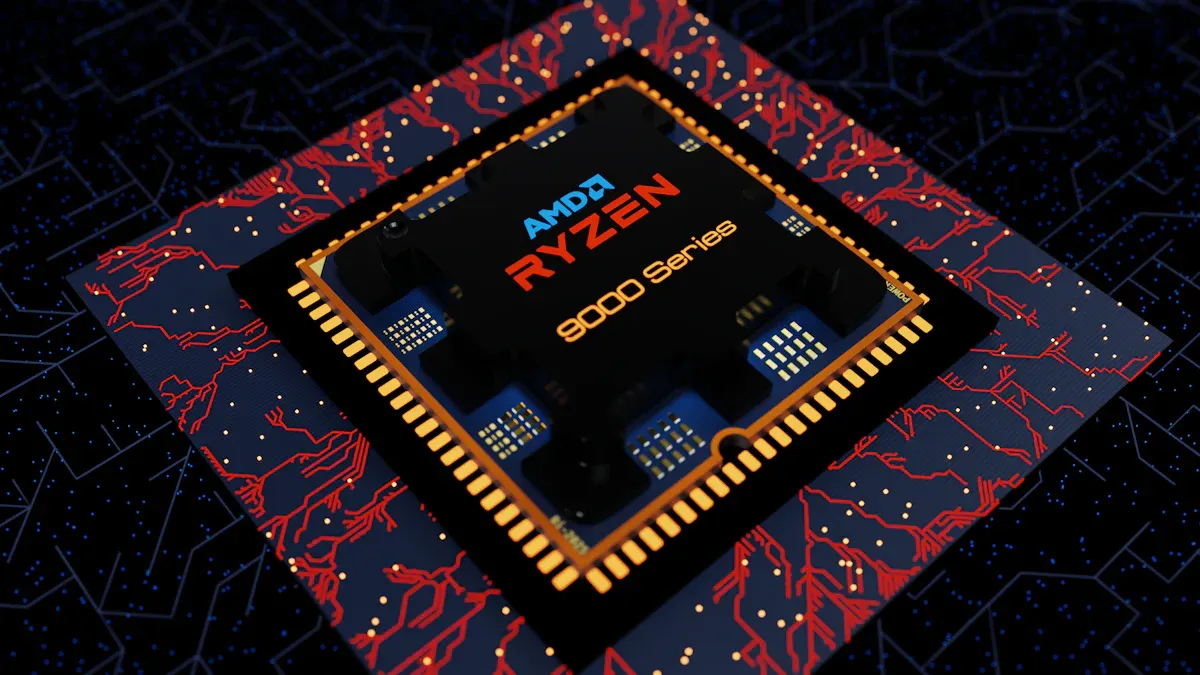
Advancements in material science have revolutionized the development of AI chiplet lead frames. Composites and alloys now play a pivotal role in meeting the demands of high-performance semiconductor applications. By combining multiple materials, manufacturers can achieve properties that surpass those of traditional metals like copper and aluminum.
Custom QFN/QFP Lead Frames: These designs incorporate ultra-fine leads to support high-density chip architectures. They integrate thermal dissipation features, ensuring reliable operation for AI processors under continuous heavy loads.
Fabrication Techniques: Laser-assisted fine stamping enables the creation of ultra-fine pitch lead frames. This innovation enhances signal integrity and power distribution, critical for complex integrated circuits (ICs).
Embedded Heat Spreaders: Multi-layered lead frame designs now include embedded heat spreaders. These features improve cooling efficiency, allowing AI chiplets to maintain optimal performance during intensive computing tasks.
The reliability and longevity of AI chiplet lead frames depend on these advancements. By leveraging composites and alloys, you can ensure your semiconductor devices withstand the rigors of long-term applications while delivering consistent performance.
Precision Etching Techniques
Precision etching techniques have transformed the manufacturing of AI chiplet lead frames. These methods allow for the creation of intricate patterns on silicon wafers, enabling the miniaturization and heterogeneous integration of components.
Reactive ion etching (RIE), inductively coupled plasma (ICP) etching, and atomic layer etching (ALE) are among the most advanced techniques used today. ALE, in particular, offers atomic-level precision, enhancing the material properties of lead frames. This precision ensures uniformity and reliability, which are essential for high-performance AI chiplets.
BonySN’s Precision Etching technology exemplifies the cutting-edge capabilities of modern manufacturing. With roll-to-roll continuous etching, you can achieve zero burr precision products with a maximum accuracy of ±0.005mm. This process eliminates the need for mold opening, streamlining sample creation and prototyping.
The benefits of advanced etching techniques extend beyond precision. Real-time control of deposition and etching rates minimizes micro-defects, improving yield rates significantly. For instance, TSMC reported a 40% reduction in defect rates and a 20% improvement in chip yield due to these innovations. By adopting such techniques, you can optimize production efficiency and ensure the highest quality for your semiconductor products.
International collaborations further accelerate the development of new lead frame materials. These partnerships enable companies to share expertise, optimize supply chains, and invest in advanced materials. By fostering innovation, they pave the way for breakthroughs in miniaturization and thermal management, essential for AI chiplets.
Incorporating these innovations into your manufacturing processes will position your products at the forefront of semiconductor technology. With precision etching and advanced materials, you can meet the demands of modern AI applications while driving efficiency and reliability.
Performance Implications
Thermal Management
Effective thermal management is crucial for the performance of AI chiplet lead frames. As chiplets operate at higher speeds and densities, they generate significant heat. If not managed properly, this heat can lead to thermal distortion, impacting the reliability and longevity of semiconductor devices.
You can mitigate these risks by selecting materials with superior thermal conductivity. For instance, copper remains a top choice due to its high thermal conductivity, which allows for efficient heat dissipation. However, advancements in composite materials also offer promising alternatives. These materials can provide enhanced thermal performance while reducing weight and cost.
Consider the following table that outlines how different materials impact thermal management:
Material Type | Thermal Conductivity (W/(m·K)) | Impact on Thermal Management |
|---|---|---|
Copper | 401 | Excellent heat dissipation; ideal for high-performance applications. |
Aluminum | 237 | Lightweight and cost-effective; suitable for budget-sensitive projects. |
Composites | Varies | Tailored properties for specific applications; can enhance thermal performance. |
By leveraging these materials, you can enhance the thermal management of your AI chiplet lead frames, ensuring optimal performance even under heavy loads.
Electrical Efficiency
Electrical efficiency is another critical factor influenced by the choice of materials in AI chiplet lead frames. The right materials can significantly improve signal integrity and reduce power consumption, which is essential for high-performance semiconductor applications.
The following table illustrates how different material types affect signal integrity and power consumption:
Material Type | Examples | Impact on Signal Integrity and Power Consumption |
|---|---|---|
Substrate Materials | FR-4, BT, Glass, Silicon Interposers | Different CTE, loss tangent, and cost profiles; glass offers superior stability and finer pitch capabilities. |
Interconnect Materials | Copper Pillars, Micro-bumps, Hybrid Bond Pads | Copper-to-copper bonding enables sub-10μm pitch, reducing resistance and improving signal integrity. |
Material Challenges | CTE Mismatch, Moisture Sensitivity, Dielectric Loss, Thermal Conductivity | Mechanical stress, moisture absorption, and inadequate heat transfer degrade performance and reliability. |
Innovative materials and techniques can enhance electrical efficiency. For example, arranging chips in three-dimensional structures can significantly boost speed. Direct connections between chips reduce power consumption, while simplifying multi-function devices into a single package improves overall chip performance.
By focusing on these aspects, you can ensure that your AI chiplet lead frames not only meet but exceed the demands of modern applications. The integration of advanced materials and innovative designs will lead to improved performance, reliability, and efficiency in your semiconductor products.
Future Trends in Packaging
Predictions for Material Developments
The future of advanced semiconductor packaging lies in the evolution of materials and techniques that address the growing complexity of chiplets. Industry reports highlight several key areas of development:
Key Areas of Development | Description |
|---|---|
Technological Innovation | Advanced materials for improved thermal and electrical performance. |
Sustainability | Eco-friendly materials and practices to reduce environmental impact. |
Advanced Packaging Solutions | Sophisticated designs to support complex architectures like 2.5D and 3D packages. |
Reliability and Qualification | Enhanced processes to ensure durability in critical applications. |
Market Growth Scenarios | Moderate growth with potential breakthroughs in materials science. |
High-purity copper substrates are expected to dominate due to their superior thermal conductivity and electrical efficiency. These substrates, combined with composite materials, will enable better thermal management and high-density connections in 3D IC packaging. Additionally, panel-level fan-out RDL-first packaging is gaining traction for its ability to support heterogeneous integration and scalability.
Sustainability will also play a pivotal role. Manufacturers are increasingly adopting panel-level advanced packaging techniques to minimize waste and energy consumption. This shift aligns with the industry’s focus on reducing the environmental footprint of wafer-level packaging processes.
Impact on AI Applications
Material advancements are set to revolutionize the scalability and integration of AI chiplets. By improving interconnect technologies, you can achieve better performance and efficiency in AI-driven applications. For example:
Thermal Management: Enhanced materials like high-purity copper and composites address heat dissipation challenges, ensuring reliable operation in power-sensitive environments.
Heterogeneous Integration: New packaging solutions, such as fan-out wafer-level packaging, facilitate the seamless integration of multiple chiplets on a single silicon wafer.
Die-to-Die Communication: Innovations in die-to-die technologies reduce latency and power loss, critical for AI workloads.
The emerging chiplet approach, supported by advancements in 3D packages, enables the creation of compact, high-performance devices. These innovations are particularly impactful in AI applications requiring real-time processing and extreme computational power.
BonySN’s expertise in precision etching and thermal management positions it as a leader in addressing these challenges. By leveraging its roll-to-roll continuous etching technology, you can achieve unparalleled precision and efficiency in manufacturing AI chiplet lead frame materials. This capability ensures your products meet the demands of modern AI applications while maintaining cost-effectiveness.
In the coming years, the combination of material innovations and advanced semiconductor packaging techniques will redefine the possibilities for AI chiplets. By staying ahead of these trends, you can unlock new opportunities in AI, HPC, and other high-growth markets.
Selecting the right ai chiplet lead frame materials is essential for advancing semiconductor technology. These materials influence thermal management, electrical efficiency, and overall performance. By leveraging innovations like precision etching and advanced composites, you can optimize silicon-based designs and enhance wafer-level packaging. BonySN’s expertise in precision manufacturing ensures your products meet the demands of modern applications. As the industry evolves, adopting cutting-edge materials and techniques will position you to lead in AI and semiconductor advancements.
FAQ
What are AI chiplet lead frames, and why are they important?
AI chiplet lead frames are structural components that connect silicon-based chips to external circuits. They play a critical role in ensuring electrical efficiency, thermal management, and overall performance in semiconductor devices.
How does material selection impact AI chiplet performance?
The choice of materials directly affects thermal conductivity, electrical efficiency, and durability. For instance, using high-purity copper or advanced composites can enhance heat dissipation and signal integrity, ensuring optimal performance for silicon-based designs.
What makes BonySN’s Precision Etching technology unique?
BonySN’s Precision Etching technology offers unmatched accuracy, achieving tolerances as fine as ±0.005mm. This process supports silicon-based applications by enabling intricate designs without mold opening, streamlining prototyping and production.
How does silicon influence AI chiplet packaging?
Silicon serves as the foundation for chiplets, enabling high-density integration and efficient electrical pathways. Advanced packaging techniques optimize silicon utilization, improving performance and scalability for AI applications.
What trends are shaping the future of AI chiplet materials?
Emerging trends include the use of high-purity copper, composite materials, and sustainable practices. These innovations enhance thermal management and electrical efficiency, ensuring silicon-based devices meet the demands of next-generation AI technologies.
See Also
Innovative Die-Free Plating Method for AI Semiconductor Development
Breakthrough Die-Less Plating Technology Speeds Up Prototyping
Moldless Selective Plating Solutions for Malaysia’s Semiconductor Industry
Die-Free Plating Services for U.S. AI and Medical Connectors
The Impact of Selective Electroplating on Lead Frame Excellence