
High-precision photochemical machining is very important for AI hardware. This technology helps makers create detailed designs with great accuracy. In making semiconductors, precision is very important. You need parts that fit well and work reliably. Using precision metal chemical etching helps you meet these standards. As you learn about AI hardware, knowing the benefits of this machining process can help you see its effect on today’s technology.
Key Takeaways
Photochemical machining is very important for making exact semiconductor parts. This helps them fit well and work reliably.
The etching process has many steps. These include coating with photoresist and developing it. This leads to high-quality metal parts without burrs.
Precision metal chemical etching allows for different material thicknesses. This helps create complex parts made for specific needs.
This technology improves AI hardware performance. It stops electrical problems and makes the whole system more reliable.
Future trends in photochemical machining include automation and eco-friendly chemicals. These will make precision and efficiency in semiconductor manufacturing even better.
What is Photochemical Machining?
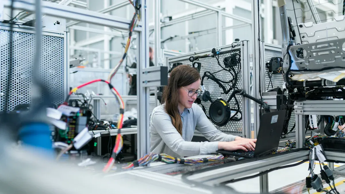
Photochemical machining (PCM) is a careful way to make things. It is very important for semiconductors. This method helps you make detailed designs on metal surfaces very accurately. It uses chemical reactions and photolithography to get the results you want.
The Etching Process
The etching process in photochemical machining has several main steps:
Photo-tool and substrate preparation: First, you get the photo-tool and substrate ready. This means adding dimension compensation for temperature and humidity changes.
Photoresist coating: Next, you put a light-sensitive material called photoresist on the substrate.
Exposure: Then, you expose the photoresist to ultraviolet light. You can use different methods, like contact or projection, based on how clear you need it.
Development: After exposure, you develop the photoresist. This reveals areas that will be etched.
Etching: The substrate goes through etching. Solvents or fast gas streams dissolve the areas that are not protected.
Photoresist stripping: Finally, you take off the leftover photoresist layer using solvents or plasma ashing. This makes sure the final product is ready for more processing.
This process helps create very precise, burr-free metal parts. These parts are important for semiconductor and microelectronics packaging.
Key Materials Used
In photochemical machining, certain materials are very important for high precision. Here are some key chemicals used:
Chemical Name | Role in Etching | CAS Number |
|---|---|---|
Hydrochloric Acid | Used for precise etching of copper and stainless steel | 7647-01-0 |
Potassium Iodide | Good gold etchant, controls material removal | 7681-11-0 |
Phosphoric Acid | Helps remove material while protecting some areas | 7664-38-2 |
Dichloromethane | Improves etching performance in certain uses | 75-09-2 |
Toluene | Used in material-solvent interaction etching | 108-88-3 |
These chemicals work together to make sure the etching process is effective and gives good results. The precision metal chemical etching technique can achieve tolerances of ±10–25 microns. This makes it good for the strict needs of semiconductor manufacturing.
By using photolithography, you can transfer detailed patterns onto a photoresist layer on a metal surface. This method allows for quick prototyping and design changes without needing expensive tools. This makes it cheaper for high-volume production.
Advantages of Precision Metal Chemical Etching
Zero Burr Precision
One big benefit of precision metal chemical etching is that it can achieve zero burr precision. This is very important for the reliability of AI hardware parts. Here’s how it helps performance:
Prevents electrical short circuits: Burrs can cause unwanted connections between parts. By getting rid of them, you lower the chance of failures.
Reduces interference interruptions: A smooth surface helps keep performance steady. This is crucial for AI uses that need high reliability.
Maintains accurate dimensional tolerances: Precision-etched shapes help make sure that electronic parts fit together well. This improves overall system performance.
With zero burr precision, you can trust that your parts will work as they should. This leads to more reliable AI hardware.
Versatility in Thickness
Precision metal chemical etching can handle many different thicknesses of materials. This flexibility lets you create many types of parts for specific needs. Here are some important points about material thickness:
Material thickness range: You can use materials from 0.03mm to 0.76mm thick.
Dimensional accuracy: You can achieve tolerances of ±0.13mm. This ensures your parts meet strict standards.
Minimum feature size: The technology can create features as small as 1x1mm.
Maximum dimension: You can work with materials up to 3000x1500mm. This fits various project needs.
This versatility makes precision metal chemical etching a great choice for making complex parts in AI hardware. You can quickly adjust to new demands without losing quality or precision.
By using the benefits of precision metal chemical etching, you improve the efficiency and effectiveness of your manufacturing. This technology not only speeds up production but also makes sure your AI hardware meets high performance standards.
Applications in AI Hardware
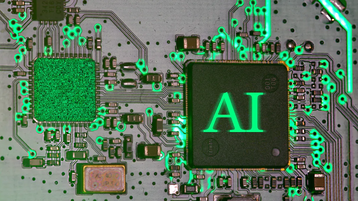
Photochemical machining is very important for different parts of AI hardware. Its accuracy and speed make it a top choice for makers. Here are some main uses:
Advanced Processors
For advanced processors, precision metal chemical etching helps create complex circuit patterns. These patterns are key for fast computing. You can get tighter tolerances, which means better performance and less power use. Many companies depend on this technology to make chips for AI tasks. For instance, a big tech company said they saw a 20% boost in processing speed after using precision etching methods.
Memory and Storage Solutions
Memory and storage solutions also gain from photochemical machining. This technology helps make high-density memory chips. You can create smaller features that hold more data in a small space. This is crucial for AI tasks that need quick data access. A recent study showed that a maker improved their memory chip yield by 30% using precision metal chemical etching. This change cut costs and boosted efficiency.
Interconnect Technologies
Interconnect technologies are another area where photochemical machining excels. It allows for making fine interconnects that connect different parts on a chip. These links must be accurate to ensure good communication between parts. By using precision etching, makers can create interconnects that reduce signal loss and improve overall performance. A user review noted how a company lowered their defect rate by 15% after using this technology in their interconnect designs.
Future Trends in Photochemical Machining
Innovations on the Horizon
As we look ahead to 2026, many exciting changes in photochemical machining will change the semiconductor industry. You can expect new ideas that will make things more precise and efficient. Here are some important trends to notice:
Laser-assisted photochemical etching: This technology will make designs more precise and faster.
Environmentally friendly chemical formulations: These new chemicals will help companies follow environmental rules while still working well.
Automation of processes: More automation will make production faster and more consistent.
AI-driven process optimization: Using AI will help improve etching settings, which will lower mistakes and boost quality.
These changes will not only improve photochemical machining but also meet the growing needs of the semiconductor market.
Impact on Semiconductor Quality
The new developments in photochemical machining will greatly affect semiconductor quality. You will notice improvements in several areas:
Enhanced precision: New ideas will allow for tighter tolerances, meaning better-fitting parts.
Increased yield rates: With better processes, manufacturers can expect more products, cutting down waste and costs.
Faster production times: Automation and AI will make workflows smoother, allowing for quicker project completion.
BonySN’s Precision Etching technology is important in this changing field. It can deliver zero burr precision and quick prototype development without molds. BonySN meets market needs effectively. This technology not only meets high standards but also helps you stay competitive in a fast-moving industry.
By following these trends, you can make sure your AI hardware stays up-to-date with the latest advancements in photochemical machining.
Photochemical machining is very important for improving AI hardware. This technology has many benefits:
It uses materials efficiently, with waste rates under 20%.
It allows quick changes in making semiconductors, which is key for new ideas.
It provides finished surfaces without needing extra steps, saving money.
As you think about the future, keep in mind that experts see the speed and flexibility of photochemical machining. This technology can create complex shapes and start production early without special tools. Using these advancements can greatly affect the semiconductor industry and improve AI uses.
Stay updated on these changes to make the most of photochemical machining in your projects!
FAQ
What is photochemical machining?
Photochemical machining is a way to make things with great accuracy. It uses chemicals and light-based methods to create detailed designs on metal. This process is very important for making high-quality parts for semiconductors.
How does precision metal chemical etching benefit AI hardware?
Precision metal chemical etching helps AI hardware by removing burrs completely. This makes connections reliable and lowers the chance of electrical problems. It improves how advanced processors and memory chips work.
What materials can be used in photochemical machining?
You can use different metals like stainless steel, copper alloys, and nickel. These metals help create detailed designs needed for semiconductor parts.
How does BonySN’s technology improve manufacturing efficiency?
BonySN’s etching technology makes prototypes quickly without needing molds. This saves time and money while keeping quality high. It’s perfect for fast production needs.
What future trends should we expect in photochemical machining?
Future trends include using lasers for etching, eco-friendly chemicals, and more automation. These changes will make the process more accurate and faster to meet the needs of the semiconductor industry.
See Also
Innovative Mold-Free Plating Technology for AI Semiconductor Chips
Precision Metal Etching at ±0.005mm for Semiconductor Uses
Advanced Reel-to-Reel Plating: Tool-Free Methods Boost US Tech Production
Continuous Metal Etching in KSA for Sensor Parts Production
Research Breakthrough: Die-Less Selective Plating Speeds Up Prototyping