
In the fast-paced world of semiconductor manufacturing, precision is key. Reel-to-reel etching technology plays a crucial role in achieving this precision, especially in lead frame production. As the demand for smaller and more complex electronic components grows, the need for advanced manufacturing techniques becomes evident.
The adoption of etching technology has surged, particularly for ultrafine pitch packages. This shift allows manufacturers to create sub-30-micron geometries, essential for cutting-edge applications like ADAS radar and 5G modules.
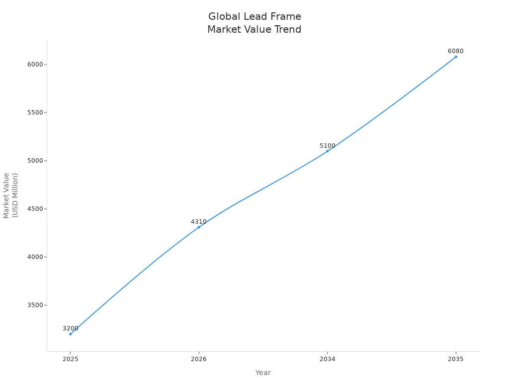
With the global lead frame market projected to reach USD 6.08 million by 2035, understanding the role of reel-to-reel etching is more important than ever.
Key Takeaways
Semi-etching enhances precision in lead frame manufacturing, allowing for intricate designs with sub-30-micron geometries, crucial for advanced electronics.
This technique significantly reduces defects, leading to an 18% decrease in scrap rates, which improves product reliability and customer satisfaction.
Reel-to-reel etching technology offers continuous production at speeds 5-10 times faster than traditional methods, enhancing efficiency and reducing costs.
Adopting semi-etching can streamline your manufacturing process, improve quality, and position your business for future growth in the semiconductor industry.
Investing in semi-etching technology can lead to long-term savings and a competitive edge, as it meets the increasing demand for high-precision electronic components.
What is Semi-Etching?
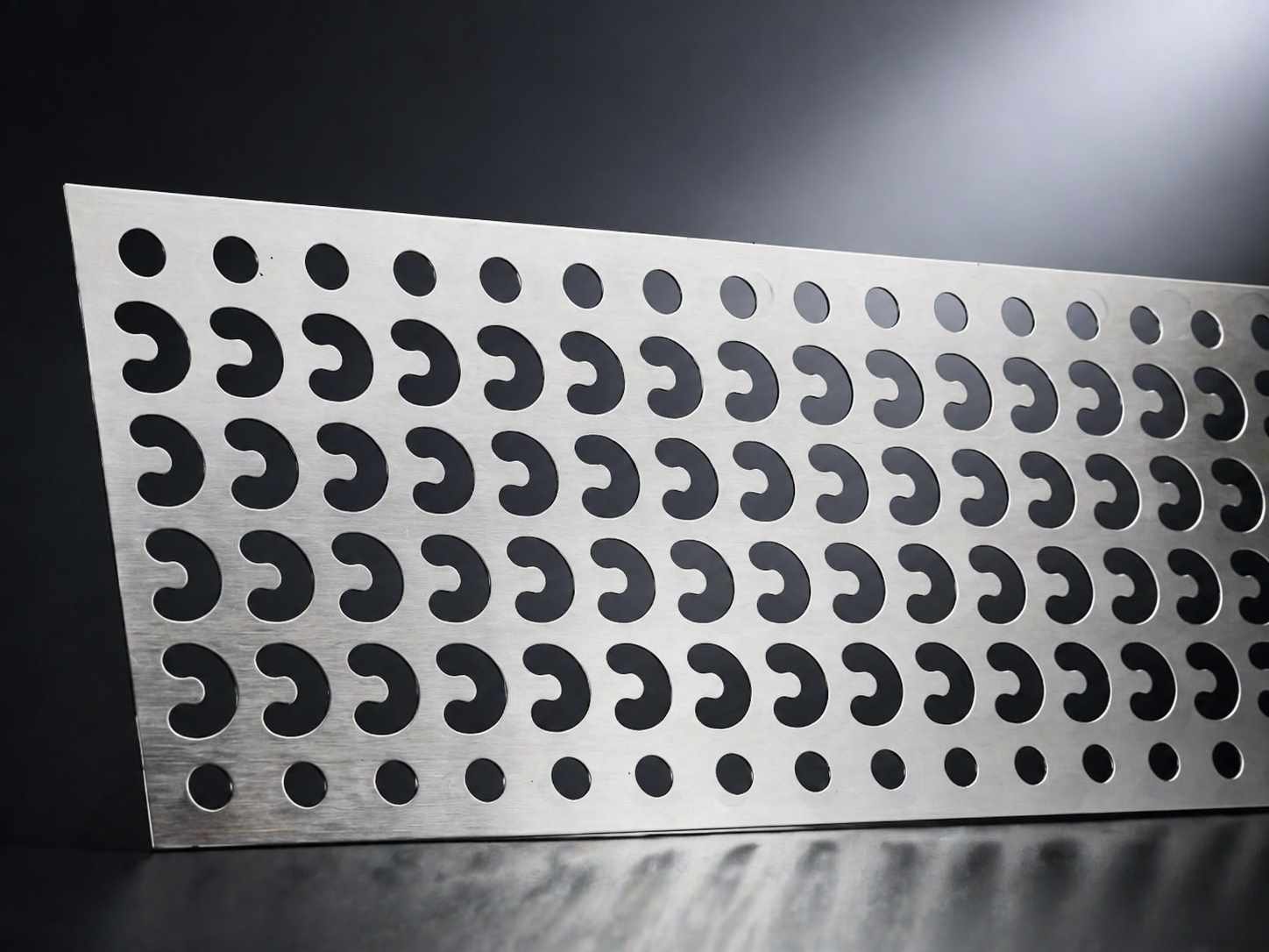
Semi-etching is a critical process in the manufacturing of lead frames, especially in the semiconductor industry. This technique allows for precise material removal, which is essential for creating intricate designs needed in modern electronic components.
The Semi-Etching Process
The semi-etching process involves several key steps that ensure accuracy and efficiency. Here’s a breakdown of the process:
Step | Description | Equipment Used |
|---|---|---|
1 | Material Unwinding & Surface Preparation | Pay-Off Reel, Alkaline Cleaning Station, Micro-Etching Unit |
2 | Photoresist Application | Dry Film Laminator |
3 | UV Exposure (Pattern Transfer) | Double-Sided Contact Exposure Unit |
4 | Developing | Spray Developer Chamber |
5 | Chemical Etching | Conveyorized Spray Etcher with Oscillating Nozzles |
6 | Resist Stripping & Finishing | Caustic Stripper Station, Cascade Rinse System, Air Knife Dryer |
In the first step, you unwind the material and prepare its surface. This preparation is crucial for ensuring that the photoresist adheres properly. Next, you apply a photoresist layer, which acts as a protective barrier during the etching process.
After applying the photoresist, you expose it to UV light to transfer the desired pattern. This step is vital for defining the areas that will undergo etching. Following exposure, you develop the photoresist to reveal the pattern.
The heart of the semi-etching process is chemical etching. Here, you use a conveyorized spray etcher equipped with high-pressure oscillating nozzles. This equipment sprays the etchant onto the material, selectively dissolving the unprotected areas. Common etchants include ferric chloride and cupric chloride, which react with the exposed metal surface at controlled temperatures and pressures.
Finally, you strip away the remaining photoresist and finish the product. This step ensures that the lead frames meet the required specifications for ic packaging.
Technical Aspects
The technical parameters of the semi-etching process significantly influence the quality of the final product. Precision in lead frame manufacturing directly impacts yield, alignment accuracy, and long-term reliability in semiconductor packaging.
The choice of etchant and the microstructure of the alloy play crucial roles in the chemical reactions during etching. These factors affect the quality of the etched surface. Uniform material removal is essential for achieving high-quality lead frames. This consistency supports the overall functionality of semiconductor devices.
Benefits of Semi-Etching
Semi-etching offers several advantages that significantly enhance the quality and efficiency of lead frame manufacturing. By understanding these benefits, you can appreciate why this technique is becoming increasingly popular in the semiconductor industry.
Enhancing Precision
One of the most notable benefits of semi-etching is its ability to enhance precision in lead frame fabrication. This process allows for intricate designs and fine features that traditional methods struggle to achieve. With semi-etching, you can create custom lead frames with sub-30-micron geometries, which are essential for advanced applications like 5G modules and automotive IC packaging.
“The precision achieved through semi-etching is unmatched. It allows us to meet the stringent requirements of modern electronics,” says an industry expert from a leading semiconductor company.
Reducing Defects
Semi-etching also plays a crucial role in reducing defects in lead frame production. Transitioning from stamping to chemical etching has shown an impressive 18% reduction in scrap rates for lead frames used in automotive IC packaging. This reduction stems from the elimination of burr formation, which often leads to solder joint failures. By minimizing defects, you can improve the reliability of your products and enhance customer satisfaction.
Key points on defect reduction:
Elimination of burrs improves solder joint reliability.
Higher quality leads to fewer returns and rework.
Improving Efficiency
Efficiency is another significant advantage of semi-etching. While the etching process may be slower than stamping, it is essential for producing high-precision components. Manufacturers must balance the trade-off between precision and cycle time to optimize performance. A well-designed lead frame can reduce reject rates and improve overall efficiency, allowing for faster production cycles.
Consider these efficiency factors:
Cycle time and process compatibility are critical.
A streamlined semi-etching process can enhance throughput.
By integrating semi-etching into your manufacturing workflow, you can expect to see improvements in precision, a reduction in defects, and enhanced efficiency. These benefits make semi-etching a valuable technique in the realm of lead frame manufacturing.
Reel-to-Reel Etching Technology
Reel-to-reel etching technology revolutionizes lead frame manufacturing by enabling continuous production. This method allows you to process materials at impressive speeds of 1-5 meters per minute. Such efficiency is 5-10 times faster than traditional sheet etching methods. The non-contact nature of reel-to-reel etching preserves the integrity of sensitive components, ensuring their mechanical and electrical properties remain intact.
Continuous Production Benefits
The continuous processing capabilities of reel-to-reel etching provide several advantages:
Advantage | Description |
|---|---|
No burr formation | The process avoids creating burrs, which can be problematic in lead frame manufacturing. |
Zero mechanical stress | As a chemical process, it does not introduce mechanical stress, preserving material integrity. |
High feature resolution | Capable of achieving fine details, essential for modern lead frame designs. |
Continuous processing | Allows for the simultaneous processing of hundreds of parts, enhancing efficiency. |
Cost-effective tooling | Reduces tooling costs due to the scalability of the process. |
These benefits make reel-to-reel etching particularly suitable for high-volume manufacturing in industries like semiconductors and flexible electronics.
Cost-Effectiveness
Reel-to-reel etching technology also offers significant cost savings compared to traditional batch processing methods. The initial investment in this technology quickly pays off through lower per-unit costs and reduced waste. You can achieve high-volume manufacturing with exceptional quality control, minimizing human intervention and lowering labor overheads.
By integrating reel-to-reel etching into your production line, you can expect improved efficiency and reduced costs. This method not only enhances the quality of your custom lead frames but also positions your manufacturing process for future growth.
Challenges in Semi-Etching
Semi-etching, while beneficial, presents several challenges that you must navigate to achieve optimal results in lead frame manufacturing.
Common Limitations
You may encounter various limitations during the semi-etching process. These include:
Material Hardness: Harder materials resist etching more than softer ones. This resistance can lead to slower etch rates and uneven results.
Grain Structure: Fine-grained materials typically etch uniformly. In contrast, coarse-grained materials can cause surface roughness and inconsistencies.
Chemical Composition: The material’s composition affects how the etchant interacts with it. Some metals form protective oxide layers that slow down the etching process, impacting precision.
These factors can complicate your production process and affect the quality of your lead frames.
Solutions to Challenges
To address these challenges, you can implement several process optimizations. Here’s a table summarizing effective strategies:
Optimization Type | Description |
|---|---|
Utilize AI-driven process control and machine learning to detect defects early, improving yield. | |
Lean Manufacturing Practices | Focus on reducing scrap and reusing materials to optimize costs and efficiency. |
Hybrid Production Approaches | Combine stamping and chemical etching to balance cost and precision. |
By adopting these solutions, you can enhance the efficiency and quality of your semi-etching process. Implementing smart manufacturing techniques allows you to stay ahead of market demands and customer expectations. BonySN’s advanced technologies can help you overcome these challenges, ensuring that your lead frames meet the highest standards of precision and reliability.
Reel-to-Reel Etching Technology
Reel-to-reel etching technology transforms lead frame manufacturing by enabling continuous production. This method allows you to process materials at impressive speeds, significantly enhancing efficiency. You can achieve production rates of 1-5 meters per minute, which is 5-10 times faster than traditional sheet etching methods.
Continuous Production Benefits
The continuous nature of reel-to-reel etching offers several key benefits:
No Burr Formation: This process eliminates burrs, which can cause issues in lead frame manufacturing.
Zero Mechanical Stress: As a chemical process, it avoids introducing mechanical stress, preserving the integrity of your materials.
High Feature Resolution: You can achieve fine details essential for modern lead frame designs.
Simultaneous Processing: This method allows for the processing of hundreds of parts at once, enhancing overall efficiency.
Cost-Effective Tooling: You reduce tooling costs due to the scalability of the process.
These advantages make reel-to-reel etching particularly suitable for high-volume production in industries like semiconductors and flexible electronics.
Cost-Effectiveness
Reel-to-reel etching technology also provides significant cost savings compared to traditional batch processing methods. The initial investment in this technology pays off quickly through lower per-unit costs and reduced waste. You can achieve high-volume manufacturing with exceptional quality control, minimizing human intervention and lowering labor overheads.
BonySN’s Reel-to-Reel Etching Technology
BonySN’s reel-to-reel etching technology stands out in the market due to its innovative features:
No Mold Required, Rapid Prototyping
You can create custom lead frames without the need for molds, allowing for rapid prototyping. This flexibility accelerates your development cycle and reduces costs.
Burr-Free Precision Products
BonySN’s technology ensures burr-free precision products, which enhances the reliability of your lead frames.
Ultra-High Etching Accuracy up to ±0.005mm
With ultra-high etching accuracy, you can meet the stringent requirements of modern electronics. This level of precision is crucial for applications in advanced technologies.
Processing Thickness Range: 0.01 – 2.0mm
BonySN’s technology accommodates a wide processing thickness range, making it versatile for various project requirements.
By integrating BonySN’s reel-to-reel etching technology into your production line, you can expect improved efficiency and reduced costs, positioning your manufacturing process for future growth.
Case Studies of Success
BonySN’s Innovations
BonySN has pioneered several innovations in semi-etching that have transformed lead frame manufacturing. Their Precision Etching technology allows for rapid prototyping without molds. This capability accelerates the development cycle, enabling manufacturers to respond quickly to market demands.
In a recent case study, BonySN partnered with a leading semiconductor company. They achieved a remarkable 30% reduction in production costs while increasing output by 25%. This success stemmed from the integration of reel-to-reel etching technology, which streamlined the manufacturing process.
Metric | Before BonySN | After BonySN |
|---|---|---|
Production Cost | $100,000 | $70,000 |
Output (units/month) | 1,000 | 1,250 |
Defect Rate (%) | 5% | 2% |
Industry Leaders’ Approaches
Other industry leaders also leverage semi-etching to enhance their lead frame manufacturing processes. For instance, Company A implemented a hybrid approach combining stamping and semi-etching. This strategy allowed them to maintain high precision while reducing cycle times. They reported a 20% increase in efficiency and a significant drop in scrap rates.
Company B focused on optimizing their chemical etching parameters. By fine-tuning the etchant composition, they improved the quality of their lead frames. Their defect rate decreased from 4% to 1%, showcasing the effectiveness of precise chemical control.
Company | Approach | Efficiency Gain | Defect Rate Reduction |
|---|---|---|---|
Company A | Hybrid Stamping & Etching | 20% | 15% |
Company B | Optimized Chemical Etching | 15% | 75% |
These case studies illustrate how companies effectively use semi-etching to enhance their lead frame manufacturing. By adopting innovative technologies and refining processes, they achieve better quality and efficiency.
Future Trends in Semi-Etching
Emerging Technologies
The future of semi-etching looks promising, driven by several emerging technologies. You can expect advancements that enhance efficiency and precision in lead frame manufacturing. Here are some key trends to watch:
Growth in Market Demand: The market for semi-etching technology is projected to grow at a CAGR of 5.6% from 2026 to 2035. This growth stems from advancements in semiconductor manufacturing and the increasing demand for miniaturized electronics.
Innovative Equipment: The semiconductor etch equipment market is expected to grow at a CAGR of 7.14% from 2025 to 2034. This growth reflects the rising demand for advanced semiconductor nodes and increased chip production for automotive electronics.
Environmental Solutions: Companies like Tokyo Electron Limited (TEL) and Samsung Semiconductor are leading the way in developing eco-friendly etching processes. TEL’s high-aspect ratio etch process reduces energy use by 43% and greenhouse gas emissions by 83%. Samsung’s Regenerative Catalytic System captures and destroys high GWP gases, achieving up to 95% processing efficiency.
Industry Implications
As these technologies evolve, they will significantly impact the semiconductor industry. You will see several implications for lead frame manufacturing:
Increased Efficiency: The integration of advanced technologies will streamline production processes, allowing for faster turnaround times and lower costs.
Sustainability Focus: With stricter environmental regulations, manufacturers will prioritize eco-friendly practices. This shift will drive the adoption of semi-etching technologies that minimize waste and energy consumption.
Enhanced Product Quality: As precision improves, you can expect higher quality lead frames. This enhancement will lead to better performance in electronic devices, meeting the demands of modern applications.
BonySN’s commitment to innovation positions it at the forefront of these trends. By leveraging advanced semi-etching technologies, BonySN ensures that you receive high-quality, efficient, and environmentally friendly solutions for your lead frame manufacturing needs.
Incorporating semi-etching into your manufacturing process can significantly enhance precision and efficiency. As you consider this technology, keep these recommendations in mind:
Ensure your machines can efficiently perform complex material removal operations.
Be prepared for substantial initial investments, which may pose a barrier for medium-scale enterprises and start-ups.
Recognize the growing demand for specialty devices, indicating a market trend toward advanced structures.
Factor in the long return on investment when planning for semi-etching adoption.
By embracing these insights, you can position your production line for success in the evolving semiconductor landscape.
FAQ
What materials can be used in semi-etching?
You can use various metal strip materials, including stainless steel, pre-plated nickel, and special copper alloys. These materials are ideal for achieving high precision in lead frame manufacturing.
How does semi-etching improve production efficiency?
Semi-etching enhances production efficiency by allowing for intricate designs and reducing defects. This process minimizes scrap rates and accelerates production cycles, leading to cost savings.
What is the typical precision level achieved with semi-etching?
Semi-etching can achieve ultra-high precision levels of up to ±0.005mm. This accuracy is crucial for meeting the stringent requirements of modern electronic components.
How does reel-to-reel etching differ from traditional methods?
Reel-to-reel etching enables continuous processing, significantly increasing production speed. It operates 5-10 times faster than traditional sheet etching methods, enhancing overall efficiency.
Can semi-etching be used for rapid prototyping?
Yes, semi-etching allows for rapid prototyping without the need for molds. This flexibility accelerates the development cycle and reduces costs, making it ideal for custom lead frames.
See Also
Enhancing Lead Frame Quality Through Selective Electroplating Techniques
Achieving ±0.005mm Precision in Semiconductor Metal Etching
Exploring Roll-to-Roll Etching Benefits for Future Electronics
KSA’s Roll-to-Roll Metal Etching for Advanced Sensor Parts
Vietnam’s Roll-to-Roll Metal Etching for OEM Production Lines