
Chemical etching is a precise manufacturing process that plays a crucial role in the production of AI server backplane connectors. As the demand for high-speed data transfer increases, you need reliable components that meet evolving signal integrity requirements. The rise in AI workloads across various industries drives this need. Organizations implement advanced machine learning and deep learning models, which require robust connectivity. In this fast-evolving landscape, chemical etching ensures you achieve high-quality, reliable backplane connectors essential for optimal performance.
Key Takeaways
Chemical etching creates precise and complex designs, making it ideal for AI server backplane connectors.
This process ensures smooth, burr-free edges and stress-free components, improving signal integrity and reliability.
Chemical etching supports a wide range of metals, offering flexibility for different performance needs in AI hardware.
Compared to stamping, chemical etching minimizes defects, reduces costs, and enhances production efficiency.
Eco-friendly etching solutions align with sustainable manufacturing trends in the tech industry.
What Is Chemical Etching?
Overview of the Process
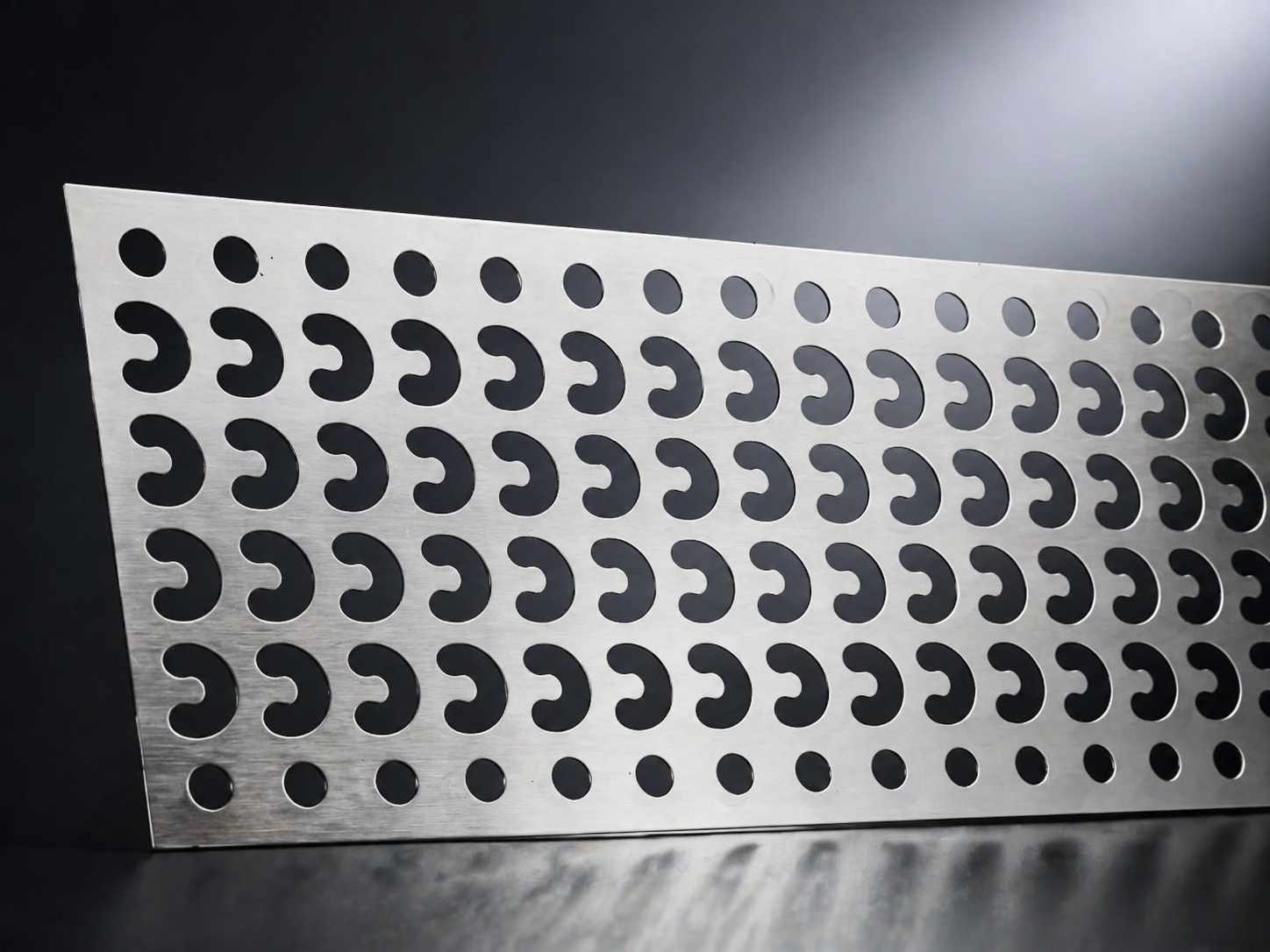
Chemical etching is a subtractive manufacturing process that allows you to create intricate designs on metal surfaces. This technique is essential for producing components with high precision and complexity, such as those used in AI server backplane connectors. The process involves several key steps:
Preparation: You begin by cleaning the substrate using chemical solutions and ultrasonic agitation, followed by rinsing with deionized water.
Photoresist Application: Next, apply a photoresist through spin coating and bake it to harden the layer.
Etching: Submerge the substrate in a chemical etchant solution to remove material from exposed areas.
Post-Etching Processes: Finally, strip the remaining photoresist, clean the substrate, and inspect the etched pattern.
This method ensures that you achieve precise and consistent results, which are crucial for maintaining the integrity of AI server components.
Key Applications in AI
In the realm of AI, chemical etching plays a pivotal role in the miniaturization of server hardware. By facilitating the integration of flexible and rigid components on printed circuit boards (PCBs), chemical etching allows you to optimize space within AI servers. This optimization enhances both reliability and performance, especially in compact environments where high-density interconnections are necessary.
The types of metals commonly used in chemical etching for electronic connectors include copper, beryllium copper, brass, phosphorous bronze, nickel/silver, steel, and stainless steel. Each metal offers unique properties that make it suitable for specific applications:
Metal Type | Properties | Applications |
|---|---|---|
Copper | Excellent electrical and thermal conductivity, corrosion resistance | Lead frames, EMI/RFI shielding, contacts, pins, terminals, connectors, bus bars |
Beryllium Copper | Highly conductive, strong, retains complex shapes | Contacts, springs |
Brass | High electrical and thermal conductivity, workable | Springs, contacts, connectors, EMI/RFI shielding, bus bars |
Phosphorous Bronze | Superior spring qualities, high fatigue resistance | Battery contacts, springs |
Nickel/Silver | High corrosion resistance, solderability | EMI/RFI shielding |
Steel | Less conductive, but can be made conductive with tin plating | EMI/RFI shielding components |
Stainless Steel | Highly resistant to moisture-related corrosion, excellent thermal conductivity | Flat springs, filters, EMI/RFI shielding and enclosures |
By choosing the appropriate metal, you can ensure that your AI server components meet the demanding requirements of modern technology.
Chemical etching not only supports the creation of complex geometries but also addresses common challenges such as poor cleaning of materials, selecting the wrong etchant, and improper mixing of etchants. By overcoming these challenges, you can achieve high-quality results that are essential for the performance of AI server backplane connectors.
Benefits of Chemical Etching for Backplane Connectors
Precision and Signal Integrity
When designing backplane connectors for industrial-grade AI server motherboard PCBs, precision is non-negotiable. Chemical etching excels in delivering unmatched accuracy, ensuring that every connector meets the stringent requirements of high-speed PCB designs. This process achieves tolerances as tight as ±0.001 inches, making it ideal for applications where signal integrity and power integrity are critical. For general applications, tolerances of ±10% of the material thickness are achievable, while thin stock materials can reach an impressive ±0.025 mm. These precise tolerances minimize impedance mismatches and reduce crosstalk, ensuring optimal performance in high-speed interconnects.
Unlike traditional fabrication methods, chemical etching eliminates the mechanical stress that can distort delicate components. This stress-free process preserves the structural integrity of connectors, which is essential for maintaining consistent signal paths in AI server environments. By ensuring uniformity and precision, chemical etching supports the development of backplane PCBs that can handle the demands of modern AI workloads.
Complex Geometries for AI Applications
AI server designs often require intricate geometries to accommodate the dense layouts of high-speed PCBs. Chemical etching enables you to create these complex shapes with ease, offering unparalleled design flexibility. Whether you need connectors with micro-scale features or components with intricate patterns, this process delivers results that other methods, such as stamping, cannot match.
The ability to work with a wide range of metals, including copper, stainless steel, and special alloys, further enhances the versatility of chemical etching. For example, copper’s excellent conductivity makes it ideal for PDN applications, while stainless steel’s corrosion resistance ensures durability in harsh environments. This adaptability allows you to tailor your designs to meet specific performance and thermal management requirements.
Chemical etching also supports selective plating techniques, such as single-sided gold plating or mold-free arbitrary local gold plating. These options enable you to enhance the functionality of your connectors without compromising on cost or efficiency. By integrating these advanced features, you can optimize your PCB design for both performance and reliability.
In addition to its technical advantages, chemical etching streamlines the assembly process. The precision of etched components reduces the need for post-fabrication adjustments, saving you time and resources. This efficiency is particularly valuable in the fast-paced world of AI server development, where rapid prototyping and production are essential.
Tip: When designing backplane connectors for AI applications, consider leveraging the precision and flexibility of chemical etching to achieve superior performance and reliability.
Chemical Etching vs. Other Methods
Advantages Over Stamping
When comparing chemical etching to stamping, you find several distinct advantages that make etching the preferred choice for manufacturing backplane connector terminals. The table below highlights key differences:
Factor | Chemical Etching | Stamping |
|---|---|---|
Edge Condition | Smooth, tapered, burr-free | Burrs, micro-tears, cold-worked |
Residual Stress | None—stress-free process | Significant—cold work zones |
Material Integrity | Fully preserved | Altered at shear edges |
Fatigue Life | Maximized—no initiation sites | Reduced by edge defects |
Chemical etching ensures minimal failure rates and produces parts that are completely flat, crucial for high-precision applications. In contrast, stamping often leads to defects and compromises part integrity. This difference is evident in the defect rates:
Process | Defect Rate | Burrs | Part Integrity |
|---|---|---|---|
Chemical Etching | Low | None | High |
Stamping | High | Common | Compromised |
Cost and Time Efficiency
Chemical etching offers significant advantages in cost optimization and time efficiency. The process allows for simultaneous processing of multiple parts on large panels, enhancing cost-effectiveness for large quantities. You can produce hundreds or even thousands of components in a single etching cycle, which is ideal for high-volume production. This scalability ensures consistency across production runs, a key differentiator from other methods that may struggle to match the same level of precision and throughput.
While the lead time for chemical etching in high-frequency PCB manufacturing can be longer due to specialized processes, the overall efficiency and reduced defect rates contribute to cost optimization. By minimizing the need for post-production adjustments, you save both time and resources, making chemical etching a cost-effective solution for producing high-quality backplane connectors.
Note: For applications requiring high precision and reliability, chemical etching provides a superior alternative to traditional stamping methods, ensuring optimal performance and cost optimization.
Real-World Applications in AI Server Technology
Case Studies of High-Performance Connectors
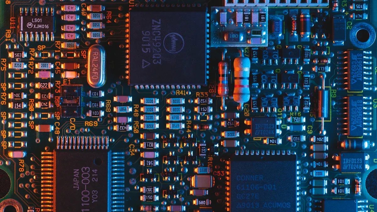
Chemical etching has proven invaluable in the development of high-performance connectors for AI servers. For instance, a leading manufacturer recently utilized chemical etching to produce connectors for an industrial-grade AI server motherboard PCB. This approach allowed them to achieve precise geometries that enhanced signal integrity and minimized crosstalk. The connectors facilitated higher data transmission speeds, meeting the increasing demands of AI workloads.
Another case involved a company specializing in AI accelerators. They adopted chemical etching to create connectors that integrated power management modules and signal repeaters. This innovation significantly improved the performance of their AI server motherboard PCB stackup, allowing for efficient thermal management and reliable connections in limited physical spaces.
Future Trends in AI Hardware Design
As AI hardware continues to evolve, several trends are shaping the adoption of chemical etching. You can expect the following developments to influence the market:
The demand for advanced semiconductor manufacturing processes is increasing, necessitating precise material removal techniques.
A notable shift towards eco-friendly practices in semiconductor manufacturing is leading to the adoption of sustainable etching chemistries.
The integration of new materials, such as tungsten, is becoming essential as AI hardware components grow more complex and energy-efficient.
Moreover, manufacturers are focusing on reducing chemical waste and hazardous emissions. This trend drives the demand for environmentally sustainable etching solutions, including recyclable acids and biodegradable formulations that comply with environmental standards.
The increasing complexity and performance requirements of AI hardware necessitate advancements in connector design and materials. As AI servers require higher data transmission speeds, the evolution of connectors will be crucial to meet these demands. Achieving reliable connections in limited physical space remains a major challenge, highlighting the need for high-quality connectors that can maintain signal integrity and minimize impedance changes.
Tip: Stay informed about these trends to leverage the advantages of chemical etching in your AI server designs.
In summary, chemical etching stands out as a vital process in the production of AI server backplane connectors. This method offers precision and flexibility, enabling you to create complex geometries essential for modern PCB designs. Compared to traditional manufacturing methods, chemical etching minimizes defects and enhances signal integrity, which is crucial for high-speed data transfer in AI applications. As AI technology continues to evolve, embracing chemical etching will ensure your server components meet the demanding requirements of the industry.
Tip: Consider the advantages of chemical etching when designing your next AI server PCB to achieve optimal performance.
FAQ
What materials can you use for chemical etching in AI connectors?
You can use metals like copper, stainless steel, brass, and beryllium copper. Each material offers unique properties that enhance performance in AI server applications.
How does chemical etching improve signal integrity?
Chemical etching provides precise geometries and smooth edges, minimizing impedance mismatches and crosstalk. This precision is crucial for maintaining high-speed data transfer in AI systems.
Is chemical etching cost-effective for large production runs?
Yes, chemical etching allows for simultaneous processing of multiple parts, making it cost-effective for high-volume production. This efficiency reduces overall manufacturing costs.
Can you achieve complex designs with chemical etching?
Absolutely! Chemical etching excels at creating intricate shapes and patterns that traditional methods struggle to replicate. This flexibility is essential for modern AI server designs.
What are the environmental benefits of chemical etching?
Chemical etching can utilize eco-friendly chemistries, reducing hazardous waste and emissions. This aligns with the growing demand for sustainable manufacturing practices in the tech industry.
See Also
High-Precision Metal Etching For Semiconductor Industry Applications
Moldless Plating Solutions For U.S. AI And Medical Connectors
Exploring Roll-To-Roll Etching And Stainless Steel For Electronics
Innovative Mold-Free Plating Technology For AI Chip Production
Moldless Plating Services For Malaysia’s Semiconductor And IC Packaging