
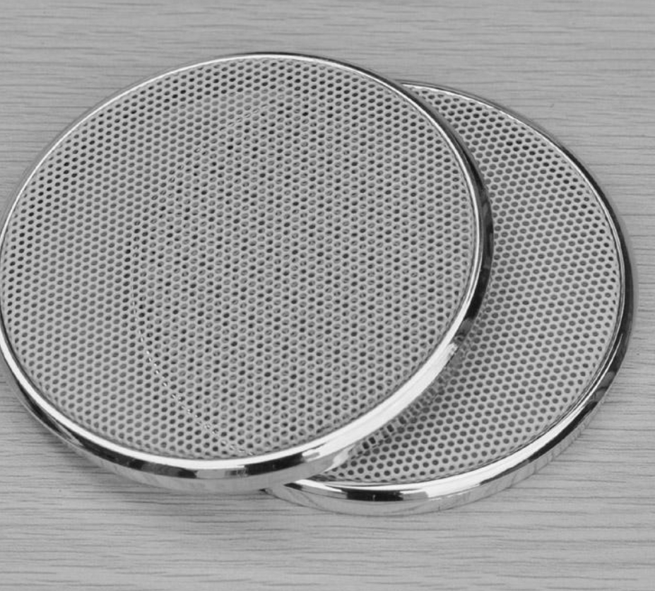
Etching removes material from surfaces. You use this fundamental process to shape various items. It boasts a long history in crafts and industries. This transformative impact on manufacturing and technology is clear. The global etch equipment sector will grow by roughly 6.5% annually over the next five years. This growth highlights the ongoing importance of etching technology and its diverse applications. You will explore its evolution and the various Applications of Etching Technology.
Key Takeaways
Etching shapes materials by removing surface layers, and this growing industry drives modern electronics production.
Modern dry etching uses specialized plasma gases to carve tiny vertical structures with supreme accuracy.
Focused laser beams vaporize specific materials to mark medical tools, heavy metals, and delicate electronics cleanly.
Chemical and laser etching processes create precise parts for surgical implants, microchips, and aerospace hardware.
Early Etching Methods and Principles
Historical Origins of Etching
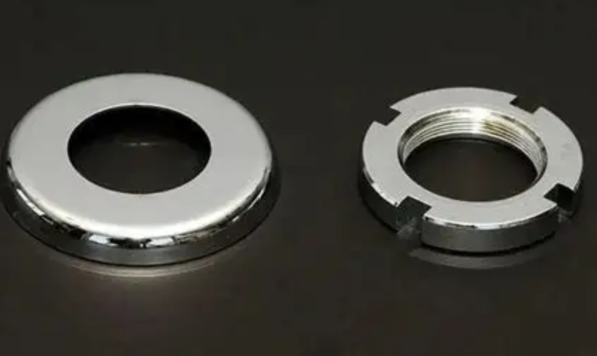
You might think etching is a modern process. However, its history stretches back thousands of years. Ancient civilizations used early forms of etching for decoration. For example, the Harappan Civilization developed techniques to etch white patterns onto carnelian beads. The Hohokam Culture in North America also practiced etching. They coated marine shells with pitch. Then, they used acid from fermented cactus juice to etch designs.
Initially, metal etching was a practical craft. You used it exclusively to decorate metal objects. Later, in the 16th century, people adapted metal etching for printmaking. Daniel Hopfer pioneered this shift in the early 1500s. Albrecht Dürer also created early print etchings. This established metal etching as a respected art form.
Basic Chemical Etching Techniques
The core principle of early etching is straightforward. You apply a protective layer, called a resist, to parts of a surface. This resist prevents the etchant from acting on those areas. Then, you expose the material to a chemical solution. This solution, the etchant, dissolves the unprotected material. You control the depth and shape of the etch by the etchant’s strength and exposure time. This basic chemical etching process formed the foundation for many applications.
Limitations of Early Methods
While effective for art and simple designs, early etching methods had significant limitations. You faced challenges with precision. These techniques struggled to create very small features. They also could not accommodate shrinking device sizes.
Challenge Category | Specific Issue | Impact / Drawback |
|---|---|---|
Precision & Feature Size | Inability to scale down | Struggles to accommodate smaller feature sizes and shrinking device geometries. |
Precision & Feature Size | Stiction | Liquid forces cause near-permanent adhesion between adjacent layers during release. |
Material Compatibility | Device geometry incompatibility | Traditional wet chemical methods fail to work effectively with modern, complex MEMS architectures. |
For example, a problem called stiction often occurred. Liquid forces caused adjacent layers to stick together permanently. Mitigating stiction required extra rinses and drying steps. This increased production time. Early chemical etching also had material compatibility issues. Some etchants, like KOH, left unwanted metal contamination. These limitations showed the need for more advanced etching technologies.
Industrial Etching and Chemical Advancements
Photochemical Etching Innovations
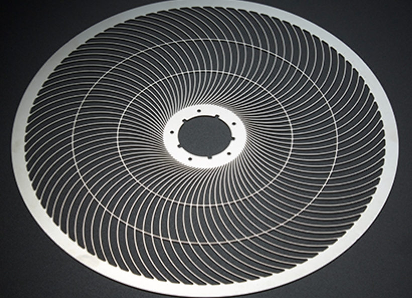
You saw the limitations of early etching methods. This led to a significant shift towards industrial applications. The development of photochemical etching marked a major breakthrough. This process became the foundational commercial method for modern photochemical metal etching. A Swedish firm, Aktiebolaget Separator, created and patented it in 1927. They used it to manufacture gap and edge filters. During World War II, this technology saw broad industrial use for hard metal parts. Modern photochemical etching directly evolved as a standalone industrial process during the 1960s. This technique initially originated as an offshoot of the printed circuit board manufacturing sector. You can now create intricate patterns and designs on various materials. This advancement made mass production of complex components possible. It revolutionized metal etching for many industries.
Precision Wet Chemical Etching
Industrial demands required more controlled and precise chemical etching processes. You needed to achieve higher precision. Modern wet chemical etching techniques deliver this. For substrate-like PCBs, you can achieve traces down to ≤ 25 µm. Dimensional or line width tolerance often exceeds ±10% variation limits. For glass substrates, etch depth accuracy is around 5%, improving over conventional 10%. When working with thin foils (less than 0.25 mm), minimum slots or openings can be as small as 0.05 mm. The dimensional tolerance for these thin foils is ±10% of the gauge, with a minimum of ±0.025 mm. Front-to-back registration is within ±0.025 mm. Thicker metal strips have tolerances from ±0.05 mm to ±0.1 mm. Depth control features offer accuracy within ±0.025 mm. This level of precision allows for the creation of highly accurate precision metal parts and fine-feature components.
Etching Technology for Microfabrication
The need for miniaturization pushed etching technology further. Microfabrication became crucial for new devices. Etching technology enables the construction of miniaturized mechanical devices. It primarily leverages batch processing techniques. Wet etching allows you to sculpt complex components from silicon quickly. This uses simple, low-cost chemical equipment. You can construct intricate three-dimensional architectures. This requires precise management of isotropic and anisotropic etch rates. Dry etching techniques provide specialized capabilities. They achieve the deeper etch profiles required for MEMS. This differs from standard integrated circuit manufacturing. This advanced metal etching is vital for modern technological progress.
Modern Etching Technologies
You have seen how etching evolved. Now, you will explore the advanced etching techniques that meet the demands of high-tech industries. These methods create complex 3D structures and extremely small features.
Dry Etching Techniques
Wet chemical etching uses liquid solutions. Dry etching, however, uses gases or plasma to remove material. This method offers significant advantages, especially in semiconductor manufacturing.
High Anisotropy: Dry etching allows directional etching. This produces straight vertical sidewalls with minimal undercutting. This is vital for modern microelectronics.
Superior Precision and Parameter Control: You can make exact adjustments. This achieves extremely fine features needed in advanced chip manufacturing. This level of precision is crucial.
Process Versatility: Dry etching offers customizable techniques. You can adapt them to a wide range of materials and specific fabrication needs.
Reduced Physical Damage: This method eliminates liquid chemicals. It prevents potential substrate damage and contamination.
Several dry etching techniques exist. Reactive Ion Etching (RIE) uses chemically reactive plasma. This plasma also has physical bombardment. Sputter etching uses inert gas ions to physically knock atoms off the surface. Vapor phase etching uses gaseous etchants. Atomic layer etching (ALE) removes material one atomic layer at a time. This offers ultimate control for creating intricate patterns.
Laser Etching Applications
Laser etching uses a focused laser beam to remove material. The laser’s energy heats the material rapidly. This causes it to vaporize or melt away. This process offers high control and can work on many materials.
You can effectively process many material types using laser etching technology:
Metals (Aluminum, Steel, Brass, Copper, Titanium): This works well for industrial components. You find these in automotive, aerospace, medical, and energy sectors.
Natural Stone (Granite, Marble): People use this for architectural elements, memorial plaques, and tombstones.
Polymers: You apply this widely across consumer goods, medical devices, commercial items, and signage.
Semiconductors: This is essential for precision marking during microelectronics manufacturing.
Ceramics: This suits broad industrial and electronic applications.
Different materials require different laser types and power settings for optimal metal etching and other applications.
Material Category | Specific Examples / Applications | Recommended Laser Type | Key Technical Feature |
|---|---|---|---|
Metals | Stainless steel, aluminum, iron | Fiber Laser | Wavelength of 1090 nm; highly absorbed by metals |
Glass | Glass surfaces | CO2 Laser | Wavelength of 10600 nm; optimal reflection and absorption |
Plastics & Resins | Fine-detailed plastic components | UV Laser | Operates at a shorter wavelength for high precision |
Industrial laser etching systems require specific power and beam characteristics.
System / Material Type | Recommended Power Range | Typical Applications |
|---|---|---|
Fiber Laser Systems | 20W to 100W | Standard metal engraving, deep etching, and high-speed marking |
CO₂ Laser Systems | 30W to 60W | General marking applications |
Stainless Steel & Aluminum | 20W to 50W | Surface marking, QR codes, serial numbers, part customization |
Brass & Copper | 30W to 50W | Fine detail engraving on reflective materials |
Titanium | 30W to 60W | High-precision aerospace and medical components |
Hard Metals (Carbon Steel) | 50W to 100W (up to 1500W+ for cutting) | Heavy tools, industrial machinery components, deep etching |
Coated / Anodized Metals | 20W to 30W | Surface layer engraving on painted or anodized parts |
Fiber laser systems feature exceptional beam quality. Their M² values approach 1.0. High focal spot power density enables deep material removal and industrial-grade etching. Precision applications rely on consistent focal spot sizes and stable beam propagation. Industrial laser etching requires balancing laser output power with dynamic pulse duration. Efficient processing of metals relies on elevated power paired with shorter pulse lengths. This induces controlled melting, vaporization, and oxidation without excessive degradation. Achieving high energy density for precision marking depends on optimizing focal spot size, mode quality, and beam divergence. This directs energy accurately onto the material target.
Electrochemical Etching
Electrochemical etching (ECE) uses an electrochemical reaction to remove material. You immerse the workpiece in an electrolyte solution. Then, you apply an electric current. This causes controlled dissolution of the material. This method is particularly useful for metal etching. It offers very controlled material removal.
Many specific applications benefit from the controlled material removal of electrochemical etching:
Semiconductor & Microelectronics: This is critical for 3D integrated circuits, through-silicon vias (TSVs), and wafer-level packaging. These require precise interconnect cavities.
MEMS Manufacturing: You use this in pressure sensors, gyroscopes, automotive accelerometers, and microfluidic channels. This ensures accurate device performance.
Medical Micro-Manufacturing: This is vital for drug delivery mechanisms, implantable devices, and diagnostic tools. It uses biocompatible materials.
Aerospace & Defense Electronics: You apply this in radar hardware, RF components, and satellite communications equipment. These require stringent quality control.
Photonics: This enables sub-micrometer precision for optical waveguides, photonic integrated circuits, and gratings. You utilize these in 5G and LiDAR systems.
Application Category | Specific Components | Key Operational Benefit |
|---|---|---|
Aerospace | Turbine blades, drive shafts, fluid pumps, generators, landing gear, fasteners | Permanent traceability without compromising structural fatigue life |
Defense & Military | Tactical aircraft parts, firearms, missile components, electronic assemblies | Compliance with strict government and defense standards |
Medical Devices | Surgical instruments, titanium bone implants, dental tools, specialized syringes | Maintains biocompatibility and strict cleanliness |
Industrial & Automotive | Heavy vehicle components, specialized machinery elements | Avoids stress concentration and dimensional changes |
Diverse Applications of Etching Technology
Etching technology has a wide-ranging impact. You find its diverse applications across many modern industries. This process is crucial for creating everything from tiny computer parts to large industrial components.
Semiconductor and Microelectronics
You rely on etching to build the complex structures inside microchips. This process defines the nanoscale features in advanced microprocessors. First, you use lithographic patterning. This involves photolithography or electron beam lithography. It selectively removes or modifies a photoresist layer. This leaves specific portions of the underlying substrate material exposed. Then, specialized etching techniques, including wet chemical etching and reactive ion etching, act upon these exposed areas. This subtractively carves and removes material from the bulk substrate. Etching generates precisely controlled, atomically accurate geometries. These are necessary for advanced microprocessors. This allows you to create the intricate circuits that power modern electronics. Etching is fundamental to the production of semiconductors and semiconductor devices. It enables the creation of smaller, more powerful microchips.
Medical Device Manufacturing
Etching plays a vital role in medical device manufacturing. You use it to create many high-precision items. Photochemical etching is a common method. It manufactures a wide array of medical devices and components. These include surgical equipment and tools like surgical blades and scalpels. You also find it in implants such as cranial implants made via titanium mesh, spinal implants, orthopedic bone devices, and dental implants. Cardiovascular and active implants like stents, pacemakers, and defibrillators also use this technology. Diagnostic and monitoring hardware, such as electron guns in MRI/CT systems, brain wave sensors, and monitoring sensor elements, benefit from etching. Medical meshes, filters, sieves, anode/cathode grids, and hearing aid elements are examples of micro-components and filters made with etching.
Medical Device Category | Etched Component | Functional Application / Highlight |
|---|---|---|
Surgical Instruments | Scalpel Blades | Achieves uniform, continuous edge sharpness |
Surgical Instruments | Microsurgical Scissors | Fabricated with tight tolerances (±2 micrometers) |
Surgical Instruments | Forceps Tips | Designed to grip tissues gently without cellular damage |
Implants & Prosthetics | Orthopedic Implants | Custom surface patterning for optimal joint contact |
Implants & Prosthetics | Cardiac Stents | Ultra-thin strut creation (down to 12 micrometers) |
Implants & Prosthetics | Dental Implants | Textured surface creation to enhance bone integration |
Medical Electronics | Pacemaker & Defibrillator Parts | Contact springs, pressure relief components, and battery terminals |
Diagnostic Equipment | Microfluidic Channels & Filters | 10-micrometer flow paths and precise filter screens for blood/cell analysis |
Diagnostic Equipment | Test Strip Contacts | Precision electrical contacts for glucose meters |
This metal etching process produces high-precision items. These include surgical needles, lancets, cutting blades, micro-separation filter screens, specialized springs, and complex electrical contacts.
Industrial and Commercial Metal Etching
You find metal etching extensively in industrial and commercial applications. It creates many different metal parts. You can etch various metals for specific uses.
Metal Category | Primary Etchant Used | Key Characteristics | Typical Applications |
|---|---|---|---|
Stainless Steels | Ferric chloride | Controlled etch rate, precise tolerances, high corrosion resistance | Aerospace, medical devices, electronics, industrial components |
Copper & Copper Alloys | Cupric chloride | Rapid etching speed, reduced undercutting, high thermal/electrical conductivity | Electrical contacts, lead frames, RF shielding, decorative items |
Nickel & Nickel Alloys | Ferric chloride | High-temperature resilience, extreme corrosion protection | Aerospace, medical implants, chemical processing, electronics |
Aluminum & Aluminum Alloys | Ferric chloride or specialized etchants | Lightweight, strong strength-to-weight ratio | Aerospace, automotive, consumer electronics |
Etching contributes significantly to the manufacture of precision metal parts. It produces functional tolerance-absorption shims. It also creates highly detailed aesthetic items like automotive interior trim. This process offers several advantages. It provides burr-free and stress-free manufacturing. It uses digital tooling and photo-resist masks. This eliminates mechanical stress, burrs, and material distortion. It keeps components perfectly flat. Etching delivers micron-level accuracy. For example, you can achieve ±10% metal thickness down to ±0.025 mm. This enables complex, intricate geometries without increasing mass. It also offers cost-effective tooling. It bypasses the need for expensive hard tooling. It avoids tool wear issues during production. This makes it ideal for high-tolerance components in industries like aerospace engineering.
Glass and Silicon Substrate Processing
You also use etching for processing glass and silicon substrates. This is crucial for display technologies and microfabrication. Etching glass substrates presents unique challenges. You must achieve high optical and mechanical quality. This requires strictly limiting surface deviation depth to ≤0.2 µm. You also control lateral undercutting to under 5 µm per 100 µm of etch depth. This involves precise balancing of laser parameters and HF etchant chemistry. Processing foldable displays with variable thickness demands engineering a smooth taper transition. This prevents stress concentrations and micro-cracks. Etching pre-bonded substrate assemblies requires uniform etchant coverage. This avoids contaminating sealed internal display cells or causing glass warpage. Processing large glass sheets necessitates protective edge taping and precise etchant layer depth control. This avoids relying on massive immersion baths. Maintaining optical haze levels below 0.5% requires suppressing preferential etching.
For silicon substrates, deep reactive ion etching (DRIE) is a primary technique. You use it in silicon substrate processing for MEMS devices. It enables high-aspect-ratio fabrication. It constructs precise vertical sidewalls (90 ±1°) with aspect ratios reaching up to 15:1. This accommodates feature sizes as small as 3µm. Etch depths range from 5µm to full through-wafer penetrations. DRIE uses a directional plasma guided by a patterned mask. This removes silicon exclusively in open mask regions. This enables 3D microstructures essential for device functionality. These include pressure sensor cavities, microfluidic channels, suspended mechanical structures, MEMS actuators and resonators, and optical MEMS components. The Bosch process is a common DRIE technique. It relies on a repeating cycle. This alternates between silicon etching and sidewall passivation. The etching phase selectively removes exposed silicon. The passivation phase protects the newly formed vertical walls. This iterative mechanism creates deep trenches, vias, cavities, and channels. They have near-vertical sidewall profiles. This advanced etching technology is vital for microfabrication.
You have seen etching evolve from an ancient craft to a sophisticated industrial process. This remarkable journey shows its continuous innovation. Etching has been a cornerstone for progress across numerous modern industries. You can expect future trends to focus on advanced automation and sustainability.
Domain
Key Technological & Process Innovations
Automation & Industry 4.0
• Deployment of AI, machine learning, and IoT sensors
• Autonomous parameter adjustments and dynamic feedbackEnvironmental Impact & Sustainability
• Transition to aqueous-based, biodegradable, and non-toxic formulations
• Adoption of plasma and laser-assisted etching processes
This ongoing development ensures the relevance and adaptability of etching technology. Its diverse applications of etching technology will continue to shape our world.
FAQ
What is the primary purpose of etching technology?
You use etching technology to remove material from a surface. This process shapes various items. It is fundamental for creating intricate designs and precise components across many industries.
How did early etching methods differ from modern techniques?
Early methods relied on basic chemical solutions and manual application of resists. You faced limitations in precision and feature size. Modern techniques use advanced chemistry, lasers, and plasma for much greater control and accuracy.
What are the main types of modern etching?
You primarily use two types: wet etching and dry etching. Wet etching uses liquid chemicals. Dry etching uses gases or plasma. Each method offers unique advantages for different materials and applications.
Where is etching most commonly used today?
You find etching crucial in semiconductor manufacturing for microchips. It is also vital for medical devices like stents and surgical tools. Industrial metal parts, glass, and silicon substrates also heavily rely on etching.
Why is dry etching important for microelectronics?
Dry etching offers high anisotropy. This means you can create straight, vertical sidewalls. This precision is essential for the tiny, complex structures in modern microchips. It also reduces contamination risks.
See Also
How Continuous Roll-To-Roll Stainless Steel Etching Shapes Future Electronics
Achieving Ultra Precise Metal Etching Standards For Advanced Semiconductor Applications
Advancing Sensor Component Manufacturing Through Metal Etching In Saudi Arabia
Streamlining Vietnam OEM Assembly Lines With Continuous Roll-To-Roll Etching
Transforming Next Generation Energy Battery Manufacturing With Continuous Etching Technology