

Free-Form electroplating revolutionizes semiconductor packaging by enhancing precision and yield, especially in rapid prototyping. This advancement is crucial for Malaysia, the sixth-largest semiconductor exporter globally. Recent statistics reveal a booming industry with 49 manufacturing projects worth RM36.1 billion approved from January to June 2024. The electrical and electronics sector, including semiconductor packaging, attracted investments totaling RM36.9 billion, over 90% of which targeted the semiconductor subsector. These developments underscore the need for innovative solutions to meet market demands and maintain Malaysia’s competitive edge.
Key Takeaways
Free-form electroplating boosts precision and yield in semiconductor packaging.
This method allows for complex designs without traditional molds, saving time and cost.
Rapid prototyping benefits from free-form electroplating, speeding up development.
Malaysia’s semiconductor industry sees significant improvements with this technology.
Adopting free-form electroplating helps companies stay competitive and innovative.
Free-Form Electroplating Principles
Electroplating Techniques
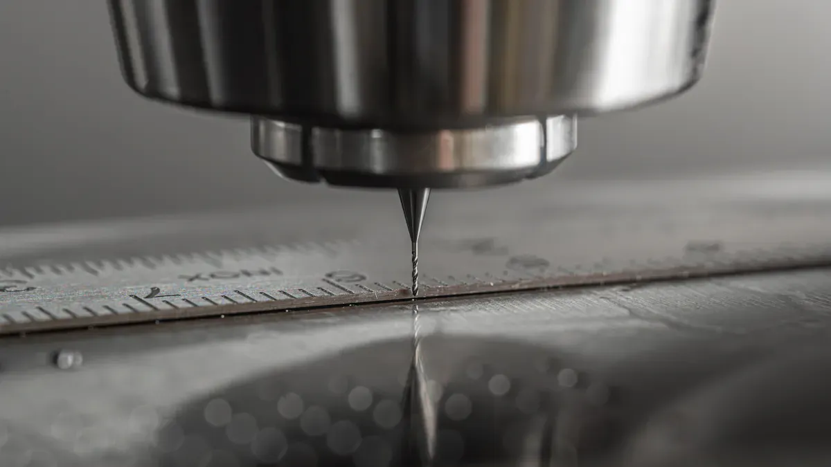
Electroplating is a process that uses electrical current to deposit a layer of material onto a substrate. This technique plays a vital role in semiconductor packaging. It allows manufacturers to create intricate designs and enhance the performance of electronic components. Here are some common electroplating techniques:
Traditional Electroplating: This method involves immersing the substrate in a solution containing metal ions. An electric current causes the metal to deposit onto the substrate.
Pulse Plating: This technique alternates between applying current and resting. It improves the quality of the deposited layer and allows for better control over thickness.
Free-Form Electroplating: This innovative approach enables you to create complex geometries and structures that traditional methods cannot achieve. It adapts to various shapes and sizes, making it ideal for modern semiconductor applications.
Mechanism of Free-Form Plating
Free-form electroplating operates on the principle of localized deposition. This means that you can control where the metal deposits on the substrate. The process begins with a conductive surface, which you prepare by cleaning and activating it. Once ready, you apply a specific voltage to the substrate while immersing it in an electrolyte solution rich in metal ions.
The key advantage of free-form electroplating lies in its ability to create complex shapes. Unlike traditional methods, which often require molds, free-form electroplating allows you to design and produce unique geometries. This flexibility is crucial in semiconductor packaging, where components often have intricate designs to meet performance requirements.
Moreover, the precision of free-form electroplating ensures that you achieve consistent results. The process can produce layers with thicknesses as fine as a few micrometers. This level of accuracy is essential for modern electronics, where even minor variations can impact performance.
Applications in Semiconductor Packaging
Rapid Prototyping Integration
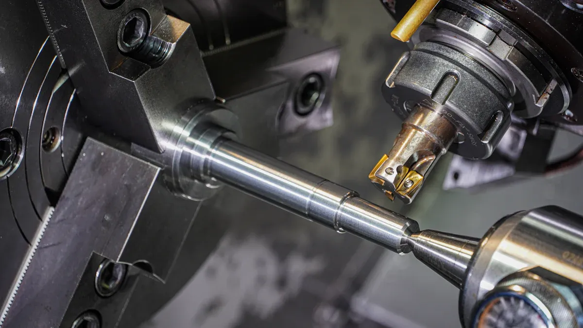
Incorporating free-form electroplating into rapid prototyping transforms how you approach semiconductor packaging. This method allows you to create prototypes quickly without the need for traditional molds. You can experiment with complex geometries and intricate designs, which are essential in modern electronics. By using free-form electroplating, you can achieve high precision and adaptability, ensuring that your prototypes meet the exact specifications required for advanced semiconductor applications. This integration not only speeds up the development process but also enhances the quality of the final product.
Case Studies in Malaysia
Malaysia’s semiconductor sector has embraced free-form electroplating, showcasing its potential through various successful implementations. For instance, a leading Malaysian semiconductor company utilized this technique to improve the efficiency of their packaging process. By adopting free-form electroplating, they reduced production time and increased yield rates significantly. This approach allowed them to meet the growing demand for high-performance electronic components.
Another notable example involves a startup in Penang that specializes in custom semiconductor solutions. They integrated free-form electroplating into their rapid prototyping workflow, enabling them to offer tailored solutions to their clients. This flexibility has positioned them as a competitive player in the market, attracting partnerships with international tech firms.
These case studies highlight the transformative impact of free-form electroplating in Malaysia’s semiconductor industry. By adopting this innovative technique, you can enhance your manufacturing capabilities and stay ahead in a rapidly evolving market.
Advantages of Free-Form Electroplating
Precision and Yield
Free-form electroplating significantly enhances precision in semiconductor packaging. This method allows you to achieve intricate designs with remarkable accuracy. You can create layers as thin as a few micrometers, which is crucial for modern electronics. The ability to control metal deposition precisely means you can minimize defects and improve overall yield rates.
Research and development initiatives in the industry focus on refining plating processes. These efforts directly address quality issues, leading to fewer defects. For instance, modifications in plating tools and automation systems help process delicate parts more effectively. As a result, you can expect improved yields and higher-quality products.
“The precision offered by free-form electroplating is unmatched. It allows us to push the boundaries of design while ensuring that our products meet the highest standards,” says an industry expert.
Cost Reduction and Efficiency
Incorporating free-form electroplating into your manufacturing process can lead to significant cost reductions. This method eliminates the need for traditional molds, which can be expensive and time-consuming to produce. By streamlining the prototyping phase, you can accelerate your time to market.
Operational efficiency also improves with free-form electroplating. The process minimizes waste by allowing for precise material usage. You can achieve higher production rates without sacrificing quality. This efficiency translates into lower defect rates and reduced rework costs.
Additionally, the flexibility of free-form electroplating enables you to adapt quickly to changing market demands. You can easily modify designs and produce small batches without incurring high costs. This adaptability positions you to respond effectively to customer needs and market trends.
Summary
By leveraging free-form electroplating, you enhance precision and yield while reducing costs and improving efficiency. This innovative approach empowers you to stay competitive in the rapidly evolving semiconductor industry.
Bonysn’s Free-Form electroplating
Precision electroplating at any location
Bonysn’s Free-Form electroplating technology stands out for its ability to deliver precision electroplating at any location on a substrate. This flexibility allows you to create intricate designs without the need for traditional molds. You can produce samples quickly, which accelerates your development process. The technology ensures zero burr precision products, achieving a remarkable film etching precision of ±0.005mm. This level of accuracy is crucial for meeting the stringent demands of the semiconductor industry.
High consistency and high yield rate
With Bonysn’s Free-Form electroplating, you can expect high consistency and yield rates. The process minimizes defects by allowing precise control over the electroplating geometry. This control eliminates overflow risks, ensuring that each layer adheres perfectly to the substrate. The technology accommodates processing thicknesses ranging from 0.01 to 2.0 mm, making it suitable for various applications. By integrating this method into your production line, you can significantly improve efficiency, reduce costs, and lower defect rates.
Rapid prototyping and mass production
Bonysn’s Free-Form electroplating excels in both rapid prototyping and mass production. The system facilitates sheet material etching with options for pre-rinse or without-rinse positioning holes. This capability streamlines subsequent processes such as stamping, bending, electroplating, and injection molding. You can adapt quickly to changing market demands, producing small batches without incurring high costs. This adaptability positions you to respond effectively to customer needs while maintaining high-quality standards.
By leveraging Bonysn’s innovative technology, you can enhance your manufacturing capabilities and stay competitive in the rapidly evolving semiconductor landscape.
Case Studies from Malaysia
Successful Implementations
In Malaysia, several companies have successfully integrated free-form electroplating into their semiconductor packaging processes. One notable example is a prominent electronics manufacturer in Selangor. They faced challenges with traditional plating methods, which often resulted in defects and longer production times. By adopting free-form electroplating, they achieved a significant reduction in defects, improving their yield rates by over 30%. This change allowed them to meet increasing market demands for high-quality components.
Another success story comes from a startup in Penang that specializes in custom semiconductor solutions. They utilized free-form electroplating to enhance their rapid prototyping capabilities. This technology enabled them to create intricate designs quickly, which attracted new clients and increased their market share. Their ability to deliver tailored solutions has positioned them as a competitive player in the industry.
Future Prospects
The future of free-form electroplating in Malaysia looks promising. As the semiconductor industry continues to grow, the demand for innovative packaging solutions will increase. Companies that adopt this technology can expect to see improvements in efficiency and product quality.
Industry experts predict that free-form electroplating will become a standard practice in semiconductor manufacturing. With ongoing advancements in technology, you can anticipate even greater precision and adaptability in the production process. As more companies recognize the benefits, the adoption of free-form electroplating will likely accelerate, driving Malaysia’s semiconductor sector to new heights.
“The integration of free-form electroplating has transformed our production capabilities. We can now respond to customer needs faster and with higher quality,” says a representative from a leading Malaysian semiconductor firm.
By embracing free-form electroplating, you position yourself to thrive in a competitive market, ensuring that your products meet the highest standards of quality and performance.
In summary, free-form electroplating plays a vital role in enhancing precision and yield in semiconductor packaging. This innovative technique allows you to create complex designs quickly and efficiently. By adopting free-form electroplating, you can improve your manufacturing processes and meet the growing demands of the market. Embracing this technology positions you to drive innovation and maintain competitiveness in Malaysia’s semiconductor industry. As the sector evolves, staying ahead with advanced solutions like free-form electroplating will be crucial for your success.
FAQ
What is free-form electroplating?
Free-form electroplating is an innovative technique that allows you to deposit metal onto specific areas of a substrate. This method enables the creation of complex geometries without traditional molds, enhancing design flexibility in semiconductor packaging.
How does free-form electroplating improve yield rates?
This technique enhances yield rates by allowing precise control over metal deposition. You can minimize defects and achieve consistent results, which leads to higher-quality products and reduced waste during manufacturing.
What materials can be used with Bonysn’s free-form electroplating?
Bonysn’s technology accommodates various materials, including stainless steel strips, pre-plated nickel, and special copper alloys. This versatility makes it suitable for a wide range of semiconductor applications.
How does free-form electroplating benefit rapid prototyping?
Free-form electroplating accelerates rapid prototyping by eliminating the need for molds. You can quickly create intricate designs, allowing for faster iterations and adjustments to meet specific project requirements.
Are there any industry standards for free-form electroplating?
Yes, free-form electroplating adheres to industry standards for quality and safety. Many companies implement rigorous testing and certification processes to ensure that their products meet the highest performance benchmarks.
See Also
Malaysia’s Semiconductor Packaging: Mold-Free Plating Solutions
U.S. AI Chip Makers Benefit From Mold-Free Plating
Strategies to Cut Plating Mold Expenses for Electronics Firms