
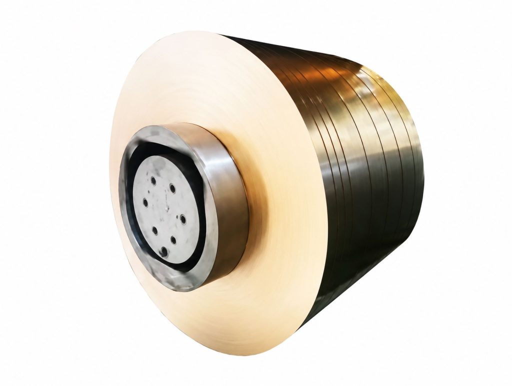
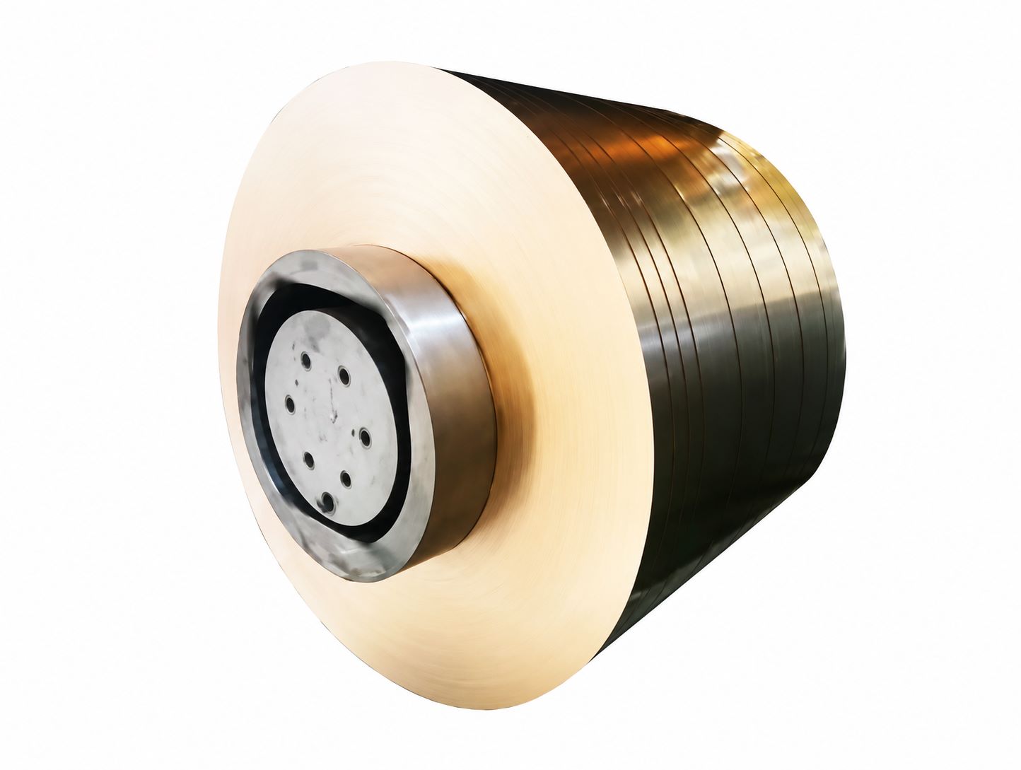
Precision plays a critical role in semiconductor manufacturing. You must understand that even minor deviations can lead to significant losses in yield. Reel-to-reel plating enhances packaging yields by ensuring consistent and accurate metal application.
Malaysia currently holds about 13% of the global market for semiconductor packaging, assembly, and testing. It ranks as the sixth largest exporter of semiconductors worldwide. The country aims to boost its market share from 7% to 14% by 2029. To achieve this, you need innovative solutions like continuous electroplating, which can help maintain a competitive edge in this rapidly evolving industry.
Key Takeaways
Precision reel-to-reel plating boosts packaging yields by ensuring consistent metal application.
Continuous electroplating enhances production efficiency and quality control in semiconductor manufacturing.
Selective plating optimizes material usage and enhances the functionality of semiconductor components.
Bonysn’s technology offers advanced electroplating techniques that improve semiconductor performance.
Investing in these technologies aligns with Malaysia’s strategic goals for semiconductor industry growth.
Electroplating Basics
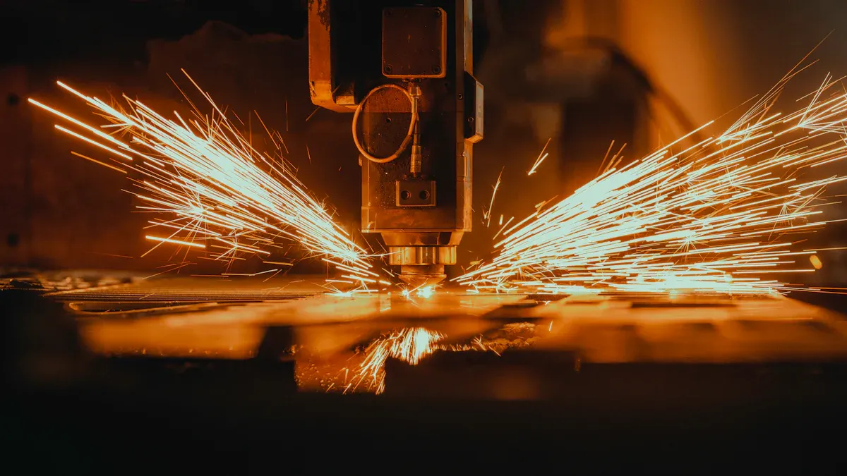
Electroplating is a manufacturing process that involves depositing a layer of metal onto a substrate. This process uses an electrochemical reaction to create a thin, uniform coating. You can think of electroplating as a way to enhance the properties of a material, making it more durable and functional.
Types of Electroplating
Several electroplating processes exist, each serving different purposes in semiconductor manufacturing. Here are some common types:
Electroplating Process | Description |
|---|---|
Traditional Electroplating | Involves depositing a thin layer of metal onto a substrate through an electrochemical reaction. |
A continuous automated process that enhances efficiency and precision in plating electronic components. | |
Allows for precise deposition of metal onto specific areas of a component, optimizing material usage. |
Importance in Semiconductor Manufacturing
Electroplating plays a vital role in semiconductor manufacturing. It contributes to the reliability and performance of semiconductor devices in several ways:
Electrical conductivity: Electroplating enhances the flow of electricity in devices.
Corrosion resistance: It protects components from environmental damage.
Solderability: Electroplating improves the ability to join components effectively.
The process begins with substrate preparation, where you clean and treat the substrate to ensure proper adhesion of the plating layer. Next, the substrate undergoes electrolysis, where it is placed in an electrolyte solution, and a direct current is applied. This initiates the electrochemical reaction, allowing metal ions to migrate to the substrate and deposit onto its surface.
In semiconductor applications, various metals are commonly used for electroplating due to their unique properties:
Gold: Known for excellent conductivity and corrosion resistance.
Silver: Offers high conductivity and is often used for its solderability.
Palladium: Provides tarnish resistance and is used in various plating applications.
Nickel: Valued for its durability and corrosion resistance.
Tin: Commonly used for soldering due to its excellent solderability.
Copper: Known for its high conductivity, making it essential in semiconductor applications.
By understanding these basics of electroplating, you can appreciate its significance in enhancing the performance and reliability of semiconductor devices.
Continuous Electroplating Advantages
Continuous electroplating offers significant benefits in semiconductor manufacturing, particularly in enhancing production efficiency and ensuring quality control. By adopting this advanced technique, you can streamline operations and achieve superior results.
Efficiency in Production
Continuous electroplating revolutionizes production by minimizing manual handling and reducing downtime. This method allows for a seamless flow of materials, boosting productivity and ensuring consistent metal deposition on lead frames. You will find that the controlled movement inherent in continuous electroplating enhances precision, reducing defects and waste. The process accommodates various shapes and sizes, making it adaptable for different applications. This flexibility translates into cost-effectiveness, optimizing material usage and reducing overall expenses.
Tip: Continuous electroplating enhances process control through real-time monitoring, allowing you to make adjustments and ensure consistent quality throughout production.
Quality Control Measures
Maintaining high standards in semiconductor manufacturing requires rigorous quality control measures. Continuous electroplating incorporates advanced techniques to ensure uniformity and precision. Here are some key measures:
Description | |
|---|---|
X-Ray Fluorescence (XRF) Analyzer | Measures the thickness of plated deposits to ensure they meet specifications. |
Elcometer | Examines the surface and structure of plated parts at a microscopic level for quality assurance. |
Glossmeter | Measures gloss and reflectivity to ensure consistent plating finishes, crucial for aesthetic appeal. |
pH Meter and Titration Equipment | Monitors acidity and alkalinity of plating solutions for optimal performance. |
Photometer | Measures color and concentration of plating solutions for precise control over the plating process. |
These tools provide you with the ability to monitor and adjust the plating process, ensuring that each component meets the required standards. By implementing these measures, you can achieve high-quality finishes that enhance the performance and reliability of semiconductor devices.
Continuous electroplating not only improves efficiency but also ensures that quality remains uncompromised. By adopting this technique, you position yourself to meet the evolving demands of the semiconductor industry, maintaining a competitive edge in Malaysia’s burgeoning market.
Reel-to-Reel Plating for Lead Frames
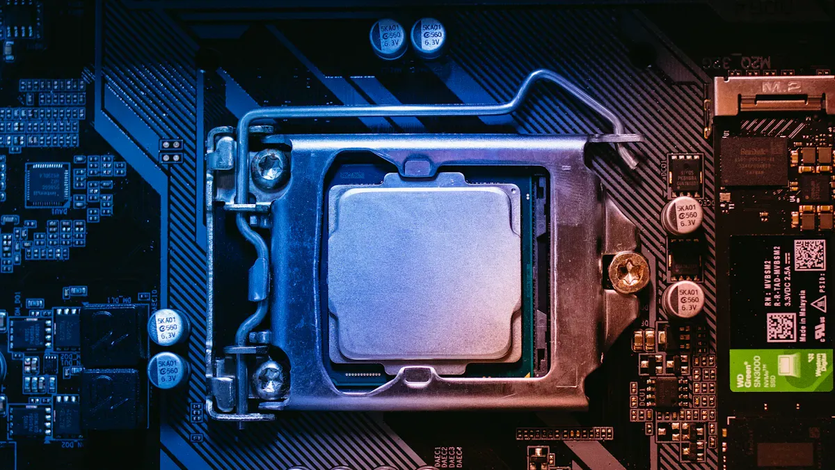
Reel-to-reel plating stands as a cornerstone in semiconductor lead frame production. This method offers several advantages that make it indispensable in the industry. By employing reel-to-reel plating, you can achieve enhanced efficiency and precision, which are crucial for maintaining high yield rates.
Selective Plating Techniques
Selective plating techniques play a pivotal role in optimizing the performance of semiconductor lead frames. These techniques allow you to apply metal coatings precisely where needed, enhancing both functionality and cost-effectiveness. Here are some of the most effective techniques:
Selective Plating Technique | Description |
|---|---|
Reel-to-Reel | A continuous process suitable for high-volume production of semiconductor lead frames. |
Barrel Plating | A method that allows for uniform plating of small parts, ideal for lead frames. |
Jigging Plating | A technique that provides precise control over the plating process, beneficial for complex lead frame designs. |
Each technique offers unique benefits, allowing you to tailor the plating process to specific requirements. For instance, reel-to-reel plating supports high-volume production, making it ideal for large-scale operations. Barrel plating ensures uniformity across small components, while jigging plating offers precision for intricate designs.
Impact on Yield Rates
The impact of reel-to-reel plating on yield rates cannot be overstated. By adopting this method, you can significantly enhance production outcomes. Here are some key advantages:
Enhanced Efficiency: The continuous flow of components reduces manual handling and downtime, boosting productivity.
Improved Precision: Consistent and accurate plating minimizes defects and waste.
Increased Flexibility: Accommodates various component shapes and sizes, reducing capital investment.
Cost-Effectiveness: Optimizes material usage and reduces labor and waste, lowering production costs.
Enhanced Process Control: Allows real-time monitoring and adjustment of process parameters for consistent quality.
Selective plating techniques further influence the electrical performance of lead frames. Controlled-depth plating ensures even coverage, while spot plating provides localized functionality. Strip plating applies a continuous metal strip, often used in connectors and contacts. Front and rear side plating optimizes material usage by restricting plating to specific surfaces.
By leveraging these techniques, you can enhance the electrical performance and reliability of semiconductor devices. Continuous electroplating, integral to reel-to-reel processes, ensures that you maintain high standards of quality and efficiency. This approach aligns with the growing demands of the semiconductor market, positioning you to meet industry challenges effectively.
Bonysn’s continuous electroplating technology
Bonysn’s continuous electroplating technology stands out in the semiconductor industry. This innovative approach offers several key advantages that enhance the performance and reliability of semiconductor components.
Precision selective electroplating
Precision selective electroplating allows you to apply metal coatings exactly where needed. This method enhances the functionality of semiconductor lead frames in various ways:
Benefit | Description |
|---|---|
Enhances the durability of semiconductor lead frames against environmental factors. | |
Solderability | Improves the ability of lead frames to bond with solder, ensuring better connections. |
Tarnish Resistance | Reduces the likelihood of surface degradation over time, maintaining performance. |
Conductivity | Increases the electrical performance of components, essential for semiconductor functionality. |
By utilizing precision selective electroplating, you can achieve ultra-high purity electroplating layers. This feature ensures that the coatings maintain their integrity over time, which is crucial for long-lasting performance.
High-precision continuous etching
High-precision continuous etching complements Bonysn’s electroplating technology. This process allows for the meticulous removal of material, ensuring that the final product meets strict specifications. You benefit from enhanced control over the etching depth and uniformity, which is vital for intricate semiconductor designs.
Roll-to-roll composite processing
Roll-to-roll composite processing is another hallmark of Bonysn’s technology. This method enables efficient production of semiconductor components by allowing continuous processing of materials. You can expect reduced waste and improved throughput, making it an ideal solution for high-volume manufacturing.
Bonysn’s commitment to innovation positions you to leverage these advanced technologies. With options like immersion gold plating, selective tin plating, and various nickel finishes, you can tailor your electroplating needs to specific applications. This flexibility ensures that you achieve the desired results without compromising quality.
Future of Continuous Electroplating in Malaysia
Technological innovations are shaping the future of continuous electroplating in Malaysia. You can expect several advancements to enhance production efficiency and environmental sustainability. Here are some key innovations:
Integration of various processes and technical know-how for product development.
Continuous R&D activities to improve plating processes.
Collaboration with customers and chemical vendors to identify the latest trends.
Development of lead-free processes, such as nickel-palladium-gold finishing.
Commitment to environmental concerns through R&D to reduce discharge.
These innovations not only improve operational efficiency but also align with global sustainability goals.
Industry Growth Potential
The growth potential for Malaysia’s semiconductor industry is significant. Continuous electroplating plays a crucial role in this expansion. The government has set strategic goals to enhance the semiconductor sector. The National Industry 4.0 Policy (NIMP 2030) and the National Semiconductor Strategy (NSS) aim to position Malaysia as a leader in the global semiconductor supply chain.
Date | Event Description | Impact on Semiconductor Industry |
|---|---|---|
12 September 2025 | X-FAB’s RM3-billion expansion of semiconductor manufacturing facility in Sarawak | Strengthens Malaysia’s position in the global semiconductor supply chain and aligns with NIMP 2030 and NSS goals. |
By investing in continuous electroplating technologies, you can enhance production capabilities and meet the growing demand for semiconductor components. This strategic alignment with national goals ensures that Malaysia remains competitive in the global market.
Embracing these advancements will not only boost your operational efficiency but also contribute to the overall growth of Malaysia’s semiconductor industry.
In summary, precision reel-to-reel plating significantly boosts packaging yields in Malaysia’s semiconductor industry. This innovative technology enhances production efficiency and quality control. By adopting continuous electroplating, you position yourself to meet the growing demands of the market.
Tip: Embrace these advancements to gain a competitive edge. The future of semiconductor manufacturing relies on your commitment to innovation and quality.
Investing in these technologies will not only improve your operations but also contribute to the overall growth of Malaysia’s semiconductor sector.
FAQ
What is reel-to-reel plating?
Reel-to-reel plating is a continuous process that applies metal coatings to electronic components. It enhances efficiency and precision in semiconductor manufacturing, ensuring consistent quality.
How does continuous electroplating improve production?
Continuous electroplating minimizes manual handling and reduces downtime. This method boosts productivity by allowing a seamless flow of materials, ensuring consistent metal deposition.
Why is selective plating important?
Selective plating applies metal coatings precisely where needed. This technique optimizes material usage and enhances the functionality of semiconductor components.
What metals are commonly used in electroplating?
Common metals include gold, silver, nickel, and copper. Each metal offers unique properties, such as conductivity and corrosion resistance, essential for semiconductor applications.
How does Bonysn’s technology benefit semiconductor manufacturing?
Bonysn’s technology offers precision selective electroplating and high-precision etching. These innovations enhance the performance and reliability of semiconductor components.
See Also
Innovative Mold-Free Plating Solutions for Malaysia’s Semiconductor Industry
Revolutionary Tool-Free Plating Boosts US Tech Manufacturing Efficiency
Advanced Mold-Free Plating for AI Chips and Medical Connectors
Cutting-Edge Mold-Free Plating for Japan’s Robotics and Connectors
Mold-Free Selective Plating for India’s Electronics and OEM Connectors