
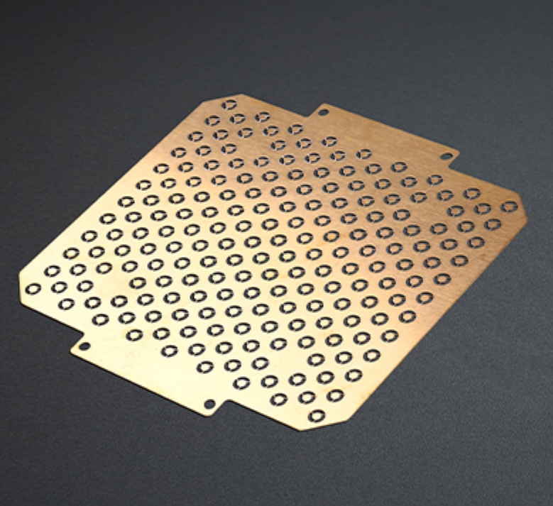
High‑Precision Electroplating for Electronic Components plays a vital role in today’s manufacturing landscape. This innovative process allows you to achieve remarkable precision, reaching up to 0.01mm in selective plating. As electronic devices become smaller and more complex, you need reliable methods that maintain quality while lowering costs. High‑Precision Electroplating for Electronic Components addresses these challenges, ensuring optimal performance and longevity for your components. Embracing this technology can significantly enhance your production capabilities and competitive edge in the market.
Key Takeaways
High-precision electroplating achieves up to 0.01mm precision, enhancing the performance and durability of electronic components.
Selective plating minimizes material usage and costs by applying coatings only to critical areas, leading to significant savings.
Advanced techniques like segmented pulse electroplating and high-resolution masking improve coating uniformity and reduce defects.
Embracing high-precision electroplating aligns with sustainability goals by reducing waste and environmental impact.
Investing in modern technologies and real-time monitoring enhances quality control and operational efficiency in electroplating processes.
Overview of High-Precision Electroplating
Importance in Electronic Components
High-precision electroplating plays a crucial role in the manufacturing of electronic components. This process allows for the precise application of metal coatings, which enhances the performance and durability of various parts. You can achieve exceptional electrical conductivity, corrosion resistance, and longevity through high-precision electroplating. These qualities are essential for ensuring that electronic components function reliably over time.
The evolution from traditional electroplating methods to high-precision techniques has transformed the industry. Traditional electroplating often resulted in inconsistent coatings and poor coverage on complex parts. In contrast, high-precision electroplating offers significant improvements in accuracy and efficiency. Here’s a comparison of the two methods:
Feature | Traditional Electroplating | High-Precision Electroplating |
|---|---|---|
Uniformity | Inconsistent | Highly Uniform |
Complex Parts | Poor Coverage | Excellent Coverage |
Build-up on Edges | Common Issue | Not an Issue |
Over the past decade, the adoption of high-precision electroplating has surged in the electronics industry. Factors driving this growth include:
The semiconductor sector’s demand for high-purity electroplating solutions for integrated circuits and chips.
The need for miniaturized electronics, which has pushed advancements in high-precision technologies.
The increasing use of renewable energy applications, particularly in solar cell technologies.
High-precision electroplating is essential for various electronic components, including circuit boards, connectors, and semiconductors. This process ensures that you achieve the necessary precision and uniformity for intricate patterns in microchips and printed circuit boards (PCBs). As a result, manufacturers can produce high-quality products that meet the demands of modern technology.
Achieving 0.01mm Precision
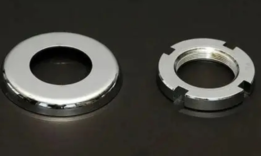
High-Resolution Masking Techniques
To achieve 0.01mm precision in electroplating, you must employ high-resolution masking techniques. These techniques ensure that the plating process only targets specific areas of the component, preventing unwanted deposits and maintaining the integrity of the design. One effective method involves using ultra-thin dry film photoresist. This material offers several advantages:
Advantage | Benefit for Plating | |
|---|---|---|
Chemical Resistance | Withstands aggressive solvents and etchants. | No degradation during plating baths. |
Adhesion | High bond strength to metal substrates. | Prevents edge lift and chemical bleed-under. |
Cure Speed | Cures with UV or visible light. | Quick readiness for plating. |
Peel Quality | Clean, tear-resistant removal. | Eliminates need for post-plating cleaning. |
By utilizing these advanced materials, you can achieve precise masking that significantly reduces electroplating defects. This precision is crucial for electronic components, where even minor inaccuracies can lead to performance issues.
Segmented Pulse Electroplating
Another key technology for achieving 0.01mm precision is segmented pulse electroplating. This method enhances the uniformity and quality of the coating by controlling the current during the electroplating process. Here’s how it works:
Low-Current Pre-Plating: This initial phase activates the substrate, improving adhesion.
Medium-Current Stable Deposition: This stage ensures uniform growth of the coating, preventing uneven thickness.
Reverse Pulse Trimming: This final step eliminates edge burrs and enhances the smoothness of the coating.
The segmented pulse electroplating process allows for real-time monitoring of coating thickness. This capability ensures that you maintain a tolerance of ±0.05μm, which is essential for stable electrical performance.
Advanced equipment plays a vital role in these processes. For instance, modern CNC machining centers provide precise control over the electroplating process, achieving micron-level tolerances. Automated assembly systems enhance efficiency and consistency, while comprehensive quality control mechanisms, including automated optical inspection, ensure dimensional accuracy and product quality.
By integrating these technologies, you can achieve the high precision required for modern electronic components while maintaining cost-effectiveness in mass production.
Cost-Effectiveness of Selective Plating
Selective plating offers significant cost savings in mass production of electronic components. By focusing on critical areas, you can minimize material usage and reduce overall production costs. Here are some key ways selective plating achieves cost-effectiveness:
Minimized Precious Metal Usage: Selective gold plating applies gold only to essential areas. This approach leads to substantial savings, as you avoid using gold in non-functional regions.
Alternative Materials for Non-Critical Areas: You can use more affordable materials like OSP (Organic Solderability Preservative) or tin plating for non-critical areas. This strategy can reduce overall material costs by as much as 28%.
Reduced Waste Generation: Selective Spot Plating significantly lowers the environmental footprint. It generates minimal chemical and waste compared to traditional full-surface plating methods. This reduction enhances operational efficiency and aligns with global compliance demands.
The economic benefits of selective plating extend beyond just material savings. Consider the following advantages:
Benefit | Description |
|---|---|
Cost Efficiency | Selective plating reduces costs by minimizing material usage and focusing on functional areas. |
Environmental Stewardship | The method enhances sustainability by reducing waste and resource consumption. |
Reduced Scrap Rates | Precise material application leads to fewer defects and less need for rework. |
In addition to these benefits, the initial investment for high-precision electroplating systems can be higher than traditional methods. For example, the setup costs for Physical Vapor Deposition (PVD) systems range from $500,000 to $5 million. However, PVD technology incurs lower operational costs over time due to reduced chemical usage, waste disposal, and energy efficiency. Modern PVD systems also enhance throughput and automation, leading to lower labor costs compared to traditional methods.
By adopting selective plating, you can achieve a balance between precision and cost, making it a smart choice for manufacturers looking to improve their bottom line while maintaining high-quality standards in electronic components.
Applications in Electronic Components

High-precision electroplating significantly enhances various electronic components. You can find its applications in several critical areas, including:
Circuit Boards: High-precision electroplating improves conductivity and prevents oxidation, ensuring reliable performance.
Connectors: This process enhances durability and corrosion resistance, making connectors more reliable in demanding environments.
Semiconductors: Precision in surface finishing is crucial for semiconductors, as it adheres to strict performance standards.
Several industries have embraced high-precision electroplating due to its benefits. The aerospace, automotive, and electronics manufacturing sectors lead the way. These industries require advanced surface finishing to improve durability, corrosion resistance, and aesthetics. For instance, in the automotive sector, high-performance components must withstand harsh conditions while maintaining functionality.
The semiconductor industry also plays a crucial role in adopting this technology. The need for precision in surface finishing drives the demand for high-quality electroplating solutions. Companies in the electronics sector benefit from enhanced product performance and durability. This improvement allows them to offer superior products, increasing their competitiveness in the market.
Challenges and Solutions
Implementing high-precision electroplating in electronic component manufacturing presents several challenges. You may encounter issues such as micro-scratches, pinholes, and uneven plating. These defects can compromise the quality of your components. Here are some common challenges you might face:
Fast oxidation: Materials like NdFeB magnets can oxidize quickly, affecting adhesion.
Brittleness and handling: Fragile structures may crack during processing.
Porosity and trapped substances: Microscopic pores can trap materials, leading to defects.
Temperature sensitivity: High temperatures can demagnetize or alter materials.
Complex geometries: Irregular shapes require precise control for uniform plating.
Hydrogen absorption: This can lead to micro-cracks and reduced performance.
Surface contamination: Debris and humidity can interfere with adhesion.
To address these challenges, manufacturers have developed innovative solutions. Advancements in chemistry and process control have transformed electroplating. Here are some effective strategies:
Real-time process monitoring: AI-driven control systems enhance consistency and reduce waste by automating adjustments.
Computer vision: Automated inspection improves defect detection and quality assurance in high-volume applications.
Digital twins: These allow for simulation and optimization of electroplating processes, reducing costs and risks.
Pulse and reverse-pulse plating: These techniques enable precise control over deposit characteristics, enhancing quality.
Environmental regulations also impact the adoption of high-precision electroplating. For instance, regulations like REACH and RoHS limit hazardous substances, affecting material choices. Stricter air quality standards can lead to increased operational costs. However, manufacturers can mitigate these impacts by investing in advanced technologies that comply with regulations while maintaining efficiency.
By understanding these challenges and implementing innovative solutions, you can enhance the effectiveness of high-precision electroplating in your production processes.
High-precision electroplating offers numerous advantages for electronic components. You achieve exceptional precision, reduced material waste, and improved production efficiency. This process not only enhances the durability and performance of your products but also aligns with sustainability goals by minimizing environmental impact.
Looking ahead, the electroplating market is set for steady growth. You can expect advancements driven by the increasing demand for electric vehicles and innovations like nanotechnology and biodegradable solutions.
Strategy | Description |
|---|---|
Cost Optimization | Innovative solutions help you save significantly on operational costs without compromising quality. |
Quality Assurance | Applying LEAN principles ensures high standards and continuous improvement. |
Process Control Optimization | Focusing on optimizing processes maintains high standards and efficiency. |
By embracing high-precision electroplating, you position yourself for success in a rapidly evolving industry.
FAQ
What is high-precision electroplating?
High-precision electroplating is a process that applies metal coatings with exceptional accuracy. You can achieve coatings as thin as 0.01mm, enhancing the performance and durability of electronic components.
How does precision strip plating work?
Precision strip plating focuses on specific areas of components. This method minimizes material usage while ensuring that only essential parts receive the coating, reducing waste and costs.
What are the benefits of selective plating?
Selective plating offers several advantages, including reduced precious metal usage, lower production costs, and improved environmental sustainability. You can achieve high-quality coatings without unnecessary waste.
Which industries benefit from high-precision electroplating?
Industries such as aerospace, automotive, and electronics manufacturing benefit significantly from high-precision electroplating. These sectors require durable, reliable components that meet strict performance standards.
How can I ensure quality in my electroplating process?
To ensure quality, implement real-time monitoring and automated inspection systems. These technologies help you maintain consistency and detect defects early in the production process.
See Also
Achieving ±0.005mm Precision In Semiconductor Metal Etching
Innovative Moldless Selective Plating For 0.009mm Gold Strips
Strategies To Lower Plating Mold Expenses For Electronics
Revolutionary Die-Free Selective Plating Speeds Up Prototyping
Moldless Selective Plating Solutions For AI And Medical Connectors